ATmega640/1280/1281/2560/2561
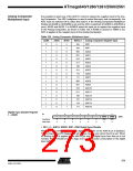
Analog Comparator
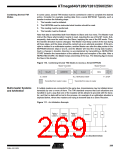
The Analog Comparator compares the input values on the positive pin AIN0 and nega-
tive pin AIN1. When the voltage on the positive pin AIN0 is higher than the voltage on
the negative pin AIN1, the Analog Comparator output, ACO, is set. The comparator’s
output can be set to trigger the Timer/Counter1 Input Capture function. In addition, the
comparator can trigger a separate interrupt, exclusive to the Analog Comparator. The
user can select Interrupt triggering on comparator output rise, fall or toggle. A block dia-
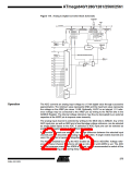
gram of the comparator and its surrounding logic is shown in Figure 113.
The Power Reduction ADC bit, PRADC, in “Power Reduction Register 0 - PRR0” on
page 54 must be disabled by writing a logical zero to be able to use the ADC input MUX.
Figure 113. Analog Comparator Block Diagram(2)
BANDGAP
REFERENCE
ACBG
ACME
ADEN
ADC MULTIPLEXER
OUTPUT(1)
Notes: 1. See Table 122 on page 273.
2. Refer to Figure 1 on page 2 and Table 38 on page 89 for Analog Comparator pin
placement.
ADC Control and Status
Register B – ADCSRB
Bit
7
–
6
ACME
R/W
0
5
–
4
–
3
MUX5
R/W
0
2
ADTS2
R/W
0
1
ADTS1
R/W
0
0
ADTS0
R/W
0
ADCSRB
Read/Write
Initial Value
R
0
R
0
R
0
• Bit 6 – ACME: Analog Comparator Multiplexer Enable
When this bit is written logic one and the ADC is switched off (ADEN in ADCSRA is
zero), the ADC multiplexer selects the negative input to the Analog Comparator. When
this bit is written logic zero, AIN1 is applied to the negative input of the Analog Compar-
ator. For a detailed description of this bit, see “Analog Comparator Multiplexed Input” on
page 273.
Analog Comparator Control
and Status Register – ACSR
Bit
7
6
ACBG
R/W
0
5
ACO
R
4
ACI
R/W
0
3
ACIE
R/W
0
2
ACIC
R/W
0
1
ACIS1
R/W
0
0
ACIS0
R/W
0
ACD
R/W
0
ACSR
Read/Write
Initial Value
N/A
• Bit 7 – ACD: Analog Comparator Disable
When this bit is written logic one, the power to the Analog Comparator is switched off.
This bit can be set at any time to turn off the Analog Comparator. This will reduce power
271
2549A–AVR–03/05

 ATMEL [ ATMEL ]