ATmega640/1280/1281/2560/2561
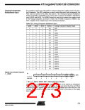
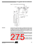
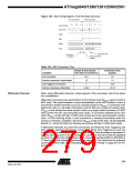
Figure 114. Analog to Digital Converter Block Schematic
ADC CONVERSION
COMPLETE IRQ
INTERRUPT
FLAGS
ADTS[2:0]
8-BIT DATABUS
15
0
ADC MULTIPLEXER SELECT
(ADMUX)
ADC CTRL & STATUS
REGISTER B (ADCSRB)
ADC CTRL & STATUS
REGISTER A (ADCSRA)
ADC DATA REGISTER
(ADCH/ADCL)
TRIGGER
SELECT
START
PRESCALER
MUX DECODER
CONVERSION LOGIC
AVCC
INTERNAL
REFERENCE
(1.1V/2.56V)
SAMPLE & HOLD
COMPARATOR
10-bit DAC
-
AREF
GND
+
SINGLE ENDED / DIFFERENTIAL SELECTION
BANDGAP (1.1V)
REFERENCE
ADC
MULTIPLEXER
OUTPUT
ADC15
ADC14
ADC13
ADC12
ADC11
ADC10
ADC9
ADC8
ADC7
ADC6
ADC5
ADC4
ADC3
ADC2
ADC1
ADC0
GAIN
AMPLIFIER
+
-
POS
INPUT
MUX
NEG INPUT
MUX
Operation
The ADC converts an analog input voltage to a 10-bit digital value through successive
approximation. The minimum value represents GND and the maximum value represents
the voltage on the AREF pin minus 1 LSB. Optionally, AVCC or an internal 1.1V refer-
ence voltage may be connected to the AREF pin by writing to the REFSn bits in the
ADMUX Register. The internal voltage reference may thus be decoupled by an external
capacitor at the AREF pin to improve noise immunity.
The analog input channel is selected by writing to the MUX bits in ADMUX. Any of the
ADC input pins, as well as GND and a fixed bandgap voltage reference, can be selected
as single ended inputs to the ADC. A selection of ADC input pins can be selected as
positive and negative inputs to the differential amplifier.
If differential channels are selected, the voltage difference between the selected input
channel pair then becomes the analog input to the ADC. If single ended channels are
used, the amplifier is bypassed altogether.
The ADC is enabled by setting the ADC Enable bit, ADEN in ADCSRA. Voltage refer-
ence and input channel selections will not go into effect until ADEN is set. The ADC
does not consume power when ADEN is cleared, so it is recommended to switch off the
ADC before entering power saving sleep modes.
275
2549A–AVR–03/05

 ATMEL [ ATMEL ]