ATmega640/1280/1281/2560/2561
Analog Comparator
Multiplexed Input
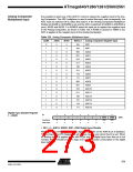
It is possible to select any of the ADC15..0 pins to replace the negative input to the Ana-
log Comparator. The ADC multiplexer is used to select this input, and consequently, the
ADC must be switched off to utilize this feature. If the Analog Comparator Multiplexer
Enable bit (ACME in ADCSRB) is set and the ADC is switched off (ADEN in ADCSRA is
zero), MUX5 and MUX2..0 in ADMUX select the input pin to replace the negative input
to the Analog Comparator, as shown in Table 122. If ACME is cleared or ADEN is set,
AIN1 is applied to the negative input to the Analog Comparator.
Table 122. Analog Comparator Mulitiplexed Input
ACME
ADEN
MUX5
MUX2..0
xxx
Analog Comparator Negative Input
0
1
1
1
1
1
1
1
1
1
1
1
1
1
1
1
1
1
x
1
0
0
0
0
0
0
0
0
0
0
0
0
0
0
0
0
x
x
AIN1
xxx
AIN1
0
0
0
0
0
0
0
0
1
1
1
1
1
1
1
1
000
001
010
011
100
101
110
111
000
001
010
011
100
101
110
111
ADC0
ADC1
ADC2
ADC3
ADC4
ADC5
ADC6
ADC7
ADC8
ADC9
ADC10
ADC11
ADC12
ADC13
ADC14
ADC15
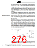
Digital Input Disable Register
1 – DIDR1
Bit
7
–
6
–
5
–
4
–
3
–
2
–
1
AIN1D
R/W
0
0
AIN0D
R/W
0
DIDR1
Read/Write
Initial Value
R
0
R
0
R
0
R
0
R
0
R
0
• Bit 1, 0 – AIN1D, AIN0D: AIN1, AIN0 Digital Input Disable
When this bit is written logic one, the digital input buffer on the AIN1/0 pin is disabled.
The corresponding PIN Register bit will always read as zero when this bit is set. When
an analog signal is applied to the AIN1/0 pin and the digital input from this pin is not
needed, this bit should be written logic one to reduce power consumption in the digital
input buffer.
273
2549A–AVR–03/05

 ATMEL [ ATMEL ]