Analog to Digital
Converter
Features
• 10-bit Resolution
• 0.5 LSB Integral Non-linearity
•
2 LSB Absolute Accuracy
• 65 - 260 µs Conversion Time
• Up to 15 kSPS at Maximum Resolution
• 16 Multiplexed Single Ended Input Channels
• 14 Differential input channels
• 4 Differential Input Channels with Optional Gain of 10x and 200x
• Optional Left Adjustment for ADC Result Readout
• 0 - VCC ADC Input Voltage Range
• Selectable 2.56V or 1.1V ADC Reference Voltage
• Free Running or Single Conversion Mode
• Interrupt on ADC Conversion Complete
• Sleep Mode Noise Canceler
The ATmega640/1280/1281/2560/2561 features a 10-bit successive approximation
ADC. The ADC is connected to an 8-channel Analog Multiplexer which allows eight sin-
gle-ended voltage inputs constructed from the pins of Port A. The single-ended voltage
inputs refer to 0V (GND).
The device also supports 16 differential voltage input combinations. Four of the differen-
tial inputs (ADC1 & ADC0, ADC & ADC2, ADC9 & ADC8 and ADC11 & ADC10) are
equipped with a programmable gain stage, providing amplification steps of 0dB (1x),
20dB (10x) or 46dB (200x) on the differential input voltage before the ADC conversion.
The 16 channels are split in two sections of 8 channels where in each section seven dif-
ferential analog input channels share a common negative terminal (ADC1/ADC9), while
any other ADC input in that section can be selected as the positive input terminal. If 1x
or 10x gain is used, 8 bit resolution can be expected. If 200x gain is used, 7 bit resolu-
tion can be expected.
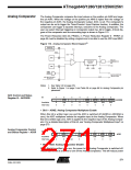
The ADC contains a Sample and Hold circuit which ensures that the input voltage to the
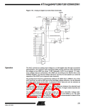
ADC is held at a constant level during conversion. A block diagram of the ADC is shown
in Figure 114.
The ADC has a separate analog supply voltage pin, AVCC. AVCC must not differ more
than 0.3V from VCC. See the paragraph “ADC Noise Canceler” on page 281 on how to
connect this pin.
Internal reference voltages of nominally 1.1V, 2.56V or AVCC are provided On-chip.
The voltage reference may be externally decoupled at the AREF pin by a capacitor for
better noise performance.
The Power Reduction ADC bit, PRADC, in “Power Reduction Register 0 - PRR0” on
page 54 must be disabled by writing a logical zero to enable the ADC.
274
ATmega640/1280/1281/2560/2561
2549A–AVR–03/05

 ATMEL [ ATMEL ]