ATmega640/1280/1281/2560/2561
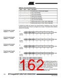
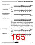
Output Compare Register 4 C
– OCR4CH and OCR4CL
Bit
7
6
5
4
3
2
1
0
OCR4C[15:8]
OCR4C[7:0]
OCR4CH
OCR4CL
Read/Write
Initial Value
R/W
0
R/W
0
R/W
0
R/W
R/W
R/W
0
R/W
0
R/W
0
0
0
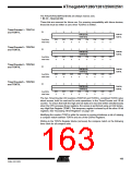
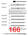
Output Compare Register 5 A
– OCR5AH and OCR5AL
Bit
7
6
5
4
3
2
1
0
OCR5A[15:8]
OCR5A[7:0]
OCR5AH
OCR5AL
Read/Write
Initial Value
R/W
0
R/W
0
R/W
0
R/W
R/W
R/W
0
R/W
0
R/W
0
0
0
Output Compare Register 5 B
– OCR5BH and OCR5BL
Bit
7
6
5
4
3
2
1
0
OCR5B[15:8]
OCR5B[7:0]
OCR5BH
OCR5BL
Read/Write
Initial Value
R/W
0
R/W
0
R/W
0
R/W
R/W
R/W
0
R/W
0
R/W
0
0
0
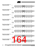
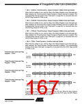
Output Compare Register 5 C
– OCR5CH and OCR5CL
Bit
7
6
5
4
3
2
1
0
OCR5C[15:8]
OCR5C[7:0]
OCR5CH
OCR5CL
Read/Write
Initial Value
R/W
0
R/W
0
R/W
0
R/W
R/W
R/W
0
R/W
0
R/W
0
0
0
The Output Compare Registers contain a 16-bit value that is continuously compared
with the counter value (TCNTn). A match can be used to generate an Output Compare
interrupt, or to generate a waveform output on the OCnx pin.
The Output Compare Registers are 16-bit in size. To ensure that both the high and low
bytes are written simultaneously when the CPU writes to these registers, the access is
performed using an 8-bit temporary High Byte Register (TEMP). This temporary register
is shared by all the other 16-bit registers. See “Accessing 16-bit Registers” on page 137.
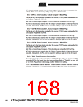
Input Capture Register 1 –
ICR1H and ICR1L
Bit
7
6
5
4
3
2
1
0
ICR1[15:8]
ICR1[7:0]
ICR1H
ICR1L
Read/Write
Initial Value
R/W
0
R/W
0
R/W
0
R/W
R/W
0
R/W
0
R/W
0
R/W
0
0
Input Capture Register 3 –
ICR3H and ICR3L
Bit
7
6
5
4
3
2
1
0
ICR3[15:8]
ICR3[7:0]
ICR3H
ICR3L
Read/Write
Initial Value
R/W
0
R/W
0
R/W
0
R/W
R/W
0
R/W
0
R/W
0
R/W
0
0
165
2549A–AVR–03/05

 ATMEL [ ATMEL ]