ATmega640/1280/1281/2560/2561
Timer/Counter0,
Timer/Counter1,
Timer/Counter3,
Timer/Counter4, and
Timer/Counter5
Prescalers
Timer/Counter0, 1, 3, 4, and 5 share the same prescaler module, but the
Timer/Counters can have different prescaler settings. The description below applies to
all Timer/Counters. Tn is used as a general name, n = 0, 1, 3, 4, or 5.
Internal Clock Source
The Timer/Counter can be clocked directly by the system clock (by setting the CSn2:0 =
1). This provides the fastest operation, with a maximum Timer/Counter clock frequency
equal to system clock frequency (fCLK_I/O). Alternatively, one of four taps from the pres-
caler can be used as a clock source. The prescaled clock has a frequency of either
fCLK_I/O/8, fCLK_I/O/64, fCLK_I/O/256, or fCLK_I/O/1024.
Prescaler Reset
The prescaler is free running, i.e., operates independently of the Clock Select logic of
the Timer/Counter, and it is shared by the Timer/Counter Tn. Since the prescaler is not
affected by the Timer/Counter’s clock select, the state of the prescaler will have implica-
tions for situations where a prescaled clock is used. One example of prescaling artifacts
occurs when the timer is enabled and clocked by the prescaler (6 > CSn2:0 > 1). The
number of system clock cycles from when the timer is enabled to the first count occurs
can be from 1 to N+1 system clock cycles, where N equals the prescaler divisor (8, 64,
256, or 1024).
It is possible to use the prescaler reset for synchronizing the Timer/Counter to program
execution. However, care must be taken if the other Timer/Counter that shares the
same prescaler also uses prescaling. A prescaler reset will affect the prescaler period
for all Timer/Counters it is connected to.
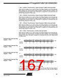
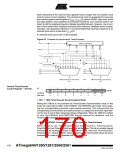
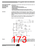
External Clock Source
An external clock source applied to the Tn pin can be used as Timer/Counter clock
(clkTn). The Tn pin is sampled once every system clock cycle by the pin synchronization
logic. The synchronized (sampled) signal is then passed through the edge detector. Fig-
ure 62 shows a functional equivalent block diagram of the Tn synchronization and edge
detector logic. The registers are clocked at the positive edge of the internal system clock
(clkI/O). The latch is transparent in the high period of the internal system clock.
The edge detector generates one clkTn pulse for each positive (CSn2:0 = 7) or negative
(CSn2:0 = 6) edge it detects.
Figure 62. Tn/T0 Pin Sampling
Tn_sync
(To Clock
Tn
D
Q
D
Q
D
Q
Select Logic)
LE
clkI/O
Synchronization
Edge Detector
The synchronization and edge detector logic introduces a delay of 2.5 to 3.5 system
clock cycles from an edge has been applied to the Tn pin to the counter is updated.
Enabling and disabling of the clock input must be done when Tn has been stable for at
least one system clock cycle, otherwise it is a risk that a false Timer/Counter clock pulse
is generated.
169
2549A–AVR–03/05

 ATMEL [ ATMEL ]