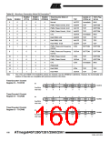
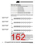
Table 83. Clock Select Bit Description
CSn2
CSn1
CSn0
Description
0
0
0
0
1
1
1
1
0
0
1
1
0
0
1
1
0
1
0
1
0
1
0
1
No clock source. (Timer/Counter stopped)
clkI/O/1 (No prescaling
clkI/O/8 (From prescaler)
clkI/O/64 (From prescaler)
clkI/O/256 (From prescaler)
clkI/O/1024 (From prescaler)
External clock source on Tn pin. Clock on falling edge
External clock source on Tn pin. Clock on rising edge
If external pin modes are used for the Timer/Countern, transitions on the Tn pin will
clock the counter even if the pin is configured as an output. This feature allows software
control of the counting.
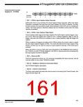
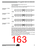
Timer/Counter1 Control
Register C – TCCR1C
Bit
7
FOC1A
W
6
FOC1B
W
5
FOC1C
W
4
–
3
–
2
–
1
–
0
–
TCCR1C
TCCR3C
TCCR4C
TCCR5C
Read/Write
Initial Value
R
0
R
0
R
0
R
0
R
0
0
0
0
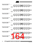
Timer/Counter3 Control
Register C – TCCR3C
Bit
7
FOC3A
W
6
FOC3B
W
5
FOC3C
W
4
–
3
–
2
–
1
–
0
–
Read/Write
Initial Value
R
0
R
0
R
0
R
0
R
0
0
0
0
Timer/Counter4 Control
Register C – TCCR4C
Bit
7
FOC4A
W
6
FOC4B
W
5
FOC4C
W
4
–
3
–
2
–
1
–
0
–
Read/Write
Initial Value
R
0
R
0
R
0
R
0
R
0
0
0
0
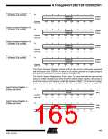
Timer/Counter5 Control
Register C – TCCR5C
Bit
7
FOC5A
W
6
FOC5B
W
5
FOC3C
W
4
–
3
–
2
–
1
–
0
–
Read/Write
Initial Value
R
0
R
0
R
0
R
0
R
0
0
0
0
• Bit 7 – FOCnA: Force Output Compare for Channel A
• Bit 6 – FOCnB: Force Output Compare for Channel B
• Bit 5 – FOCnC: Force Output Compare for Channel C
The FOCnA/FOCnB/FOCnC bits are only active when the WGMn3:0 bits specifies a
non-PWM mode. When writing a logical one to the FOCnA/FOCnB/FOCnC bit, an
immediate compare match is forced on the waveform generation unit. The
OCnA/OCnB/OCnC output is changed according to its COMnx1:0 bits setting. Note that
the FOCnA/FOCnB/FOCnC bits are implemented as strobes. Therefore it is the value
present in the COMnx1:0 bits that determine the effect of the forced compare.
A FOCnA/FOCnB/FOCnC strobe will not generate any interrupt nor will it clear the timer
in Clear Timer on Compare Match (CTC) mode using OCRnA as TOP.
162
ATmega640/1280/1281/2560/2561
2549A–AVR–03/05

 ATMEL [ ATMEL ]