ATmega640/1280/1281/2560/2561
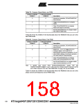
Table 81. Compare Output Mode, Phase Correct and Phase and Frequency Correct
PWM
COMnA1/COMnB/
COMnC1
COMnA0/COMnB0/
COMnC0
Description
0
0
Normal port operation, OCnA/OCnB/OCnC
disconnected.
0
1
WGM13:0 = 8, 9 10 or 11: Toggle OC1A on
Compare Match, OC1B and OC1C
disconnected (normal port operation). For all
other WGM1 settings, normal port operation,
OC1A/OC1B/OC1C disconnected.
1
1
0
1
Clear OCnA/OCnB/OCnC on compare
match when up-counting. Set
OCnA/OCnB/OCnC on compare match
when downcounting.
Set OCnA/OCnB/OCnC on compare match
when up-counting. Clear
OCnA/OCnB/OCnC on compare match
when downcounting.
Note:
A
special case occurs when OCRnA/OCRnB/OCRnC equals TOP and
COMnA1/COMnB1//COMnC1 is set. See “Phase Correct PWM Mode” on page 150. for
more details.
• Bit 1:0 – WGMn1:0: Waveform Generation Mode
Combined with the WGMn3:2 bits found in the TCCRnB Register, these bits control the
counting sequence of the counter, the source for maximum (TOP) counter value, and
what type of waveform generation to be used, see Table 82. Modes of operation sup-
ported by the Timer/Counter unit are: Normal mode (counter), Clear Timer on Compare
match (CTC) mode, and three types of Pulse Width Modulation (PWM) modes. (See
“Modes of Operation” on page 147.).
159
2549A–AVR–03/05

 ATMEL [ ATMEL ]