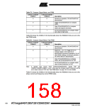
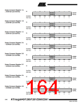
Table 82. Waveform Generation Mode Bit Description(1)
WGMn2
(CTCn)
WGMn1
WGMn0
Timer/Counter Mode of
Update of
OCRnx at
TOVn Flag
Set on
Mode
WGMn3
(PWMn1) (PWMn0) Operation
TOP
0
1
2
3
4
5
6
7
8
0
0
0
0
0
0
0
0
1
0
0
0
0
1
1
1
1
0
0
0
1
1
0
0
1
1
0
0
1
0
1
0
1
0
1
0
Normal
0xFFFF
0x00FF
0x01FF
0x03FF
OCRnA
0x00FF
0x01FF
0x03FF
ICRn
Immediate
TOP
MAX
PWM, Phase Correct, 8-bit
PWM, Phase Correct, 9-bit
PWM, Phase Correct, 10-bit
CTC
BOTTOM
BOTTOM
BOTTOM
MAX
TOP
TOP
Immediate
TOP
Fast PWM, 8-bit
TOP
Fast PWM, 9-bit
TOP
TOP
Fast PWM, 10-bit
TOP
TOP
PWM, Phase and Frequency
Correct
BOTTOM
BOTTOM
9
1
0
0
1
PWM, Phase and Frequency
Correct
OCRnA
BOTTOM
BOTTOM
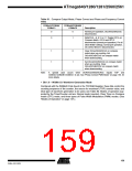
10
11
12
13
14
15
1
1
1
1
1
1
0
0
1
1
1
1
1
1
0
0
1
1
0
1
0
1
0
1
PWM, Phase Correct
PWM, Phase Correct
CTC
ICRn
OCRnA
ICRn
–
TOP
TOP
Immediate
–
BOTTOM
BOTTOM
MAX
(Reserved)
–
Fast PWM
ICRn
OCRnA
TOP
TOP
TOP
Fast PWM
TOP
Note:
1. The CTCn and PWMn1:0 bit definition names are obsolete. Use the WGMn2:0 definitions. However, the functionality and
location of these bits are compatible with previous versions of the timer.
Timer/Counter1 Control
Register B – TCCR1B
Bit
7
ICNC1
R/W
0
6
ICES1
R/W
0
5
–
4
WGM13
R/W
0
3
WGM12
R/W
0
2
CS12
R/W
0
1
CS11
R/W
0
0
CS10
R/W
0
TCCR1B
TCCR3B
TCCR4B
Read/Write
Initial Value
R
0
Timer/Counter3 Control
Register B – TCCR3B
Bit
7
ICNC3
R/W
0
6
ICES3
R/W
0
5
–
4
WGM33
R/W
0
3
WGM32
R/W
0
2
CS32
R/W
0
1
CS31
R/W
0
0
CS30
R/W
0
Read/Write
Initial Value
R
0
Timer/Counter4 Control
Register B – TCCR4B
Bit
7
ICNC4
R/W
0
6
ICES4
R/W
0
5
–
4
WGM43
R/W
0
3
WGM42
R/W
0
2
CS42
R/W
0
1
CS41
R/W
0
0
CS40
R/W
0
Read/Write
Initial Value
R
0
160
ATmega640/1280/1281/2560/2561
2549A–AVR–03/05

 ATMEL [ ATMEL ]