ATmega640/1280/1281/2560/2561
16-bit Timer/Counter
Register Description
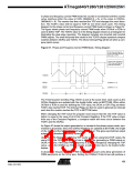
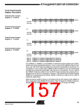
Timer/Counter1 Control
Register A – TCCR1A
Bit
7
COM1A1
R/W
6
COM1A0
R/W
5
COM1B1
R/W
4
COM1B0
R/W
3
COM1C1
R/W
2
COM1C0
R/W
1
WGM11
R/W
0
0
WGM10
R/W
0
TCCR1A
TCCR3A
TCCR4A
TCCR5A
Read/Write
Initial Value
0
0
0
0
0
0
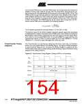
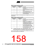
Timer/Counter3 Control
Register A – TCCR3A
Bit
7
COM3A1
R/W
6
COM3A0
R/W
5
COM3B1
R/W
4
COM3B0
R/W
3
COM3C1
R/W
2
COM3C0
R/W
1
WGM31
R/W
0
0
WGM30
R/W
0
Read/Write
Initial Value
0
0
0
0
0
0
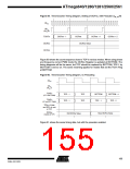
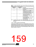
Timer/Counter4 Control
Register A – TCCR4A
Bit
7
COM4A1
R/W
6
COM4A0
R/W
5
COM4B1
R/W
4
COM4B0
R/W
3
COM4C1
R/W
2
COM4C0
R/W
1
WGM41
R/W
0
0
WGM40
R/W
0
Read/Write
Initial Value
0
0
0
0
0
0
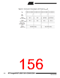
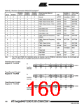
Timer/Counter5 Control
Register A – TCCR5A
Bit
7
COM5A1
R/W
6
COM5A0
R/W
5
COM5B1
R/W
4
COM5B0
R/W
3
COM5C1
R/W
2
COM5C0
R/W
1
WGM51
R/W
0
0
WGM50
R/W
0
Read/Write
Initial Value
0
0
0
0
0
0
• Bit 7:6 – COMnA1:0: Compare Output Mode for Channel A
• Bit 5:4 – COMnB1:0: Compare Output Mode for Channel B
• Bit 3:2 – COMnC1:0: Compare Output Mode for Channel C
The COMnA1:0, COMnB1:0, and COMnC1:0 control the output compare pins (OCnA,
OCnB, and OCnC respectively) behavior. If one or both of the COMnA1:0 bits are writ-
ten to one, the OCnA output overrides the normal port functionality of the I/O pin it is
connected to. If one or both of the COMnB1:0 bits are written to one, the OCnB output
overrides the normal port functionality of the I/O pin it is connected to. If one or both of
the COMnC1:0 bits are written to one, the OCnC output overrides the normal port func-
tionality of the I/O pin it is connected to. However, note that the Data Direction Register
(DDR) bit corresponding to the OCnA, OCnB or OCnC pin must be set in order to
enable the output driver.
When the OCnA, OCnB or OCnC is connected to the pin, the function of the COMnx1:0
bits is dependent of the WGMn3:0 bits setting. Table 79 shows the COMnx1:0 bit func-
tionality when the WGMn3:0 bits are set to a normal or a CTC mode (non-PWM).
157
2549A–AVR–03/05

 ATMEL [ ATMEL ]