ATmega16(L)
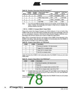
Table 41. Compare Output Mode, Phase Correct PWM Mode(1)
COM01 COM00 Description
0
0
1
0
1
0
Normal port operation, OC0 disconnected.
Reserved
Clear OC0 on compare match when up-counting. Set OC0 on compare
match when downcounting.
1
1
Set OC0 on compare match when up-counting. Clear OC0 on compare
match when downcounting.
Note:
1. A special case occurs when OCR0 equals TOP and COM01 is set. In this case, the
compare match is ignored, but the set or clear is done at TOP. See “Phase Correct
PWM Mode” on page 74 for more details.
• Bit 2:0 – CS02:0: Clock Select
The three Clock Select bits select the clock source to be used by the Timer/Counter.
Table 42. Clock Select Bit Description
CS02
CS01
CS00
Description
0
0
0
0
1
1
1
1
0
0
1
1
0
0
1
1
0
1
0
1
0
1
0
1
No clock source (Timer/Counter stopped).
clkI/O/(No prescaling)
clkI/O/8 (From prescaler)
clkI/O/64 (From prescaler)
clkI/O/256 (From prescaler)
clkI/O/1024 (From prescaler)
External clock source on T0 pin. Clock on falling edge.
External clock source on T0 pin. Clock on rising edge.
If external pin modes are used for the Timer/Counter0, transitions on the T0 pin will
clock the counter even if the pin is configured as an output. This feature allows software
control of the counting.
Timer/Counter Register –
TCNT0
Bit
7
6
5
4
3
2
1
0
TCNT0[7:0]
TCNT0
Read/Write
Initial Value
R/W
0
R/W
0
R/W
0
R/W
0
R/W
0
R/W
0
R/W
0
R/W
0
The Timer/Counter Register gives direct access, both for read and write operations, to
the Timer/Counter unit 8-bit counter. Writing to the TCNT0 Register blocks (removes)
the compare match on the following timer clock. Modifying the counter (TCNT0) while
the counter is running, introduces a risk of missing a compare match between TCNT0
and the OCR0 Register.
79
2466E–AVR–10/02

 ATMEL [ ATMEL ]