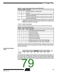
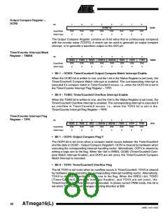
Output Compare Register –
OCR0
Bit
7
6
5
4
3
2
1
0
OCR0[7:0]
OCR0
Read/Write
Initial Value
R/W
0
R/W
0
R/W
0
R/W
0
R/W
0
R/W
0
R/W
0
R/W
0
The Output Compare Register contains an 8-bit value that is continuously compared
with the counter value (TCNT0). A match can be used to generate an output compare
interrupt, or to generate a waveform output on the OC0 pin.
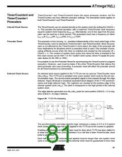
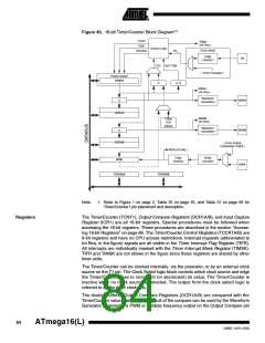
Timer/Counter Interrupt Mask
Register – TIMSK
Bit
7
OCIE2
R/W
0
6
TOIE2
R/W
0
5
TICIE1
R/W
0
4
OCIE1A
R/W
0
3
OCIE1B
R/W
0
2
TOIE1
R/W
0
1
OCIE0
R/W
0
0
TOIE0
R/W
0
TIMSK
Read/Write
Initial Value
• Bit 1 – OCIE0: Timer/Counter0 Output Compare Match Interrupt Enable
When the OCIE0 bit is written to one, and the I-bit in the Status Register is set (one), the
Timer/Counter0 Compare Match interrupt is enabled. The corresponding interrupt is
executed if a compare match in Timer/Counter0 occurs, i.e., when the OCF0 bit is set in
the Timer/Counter Interrupt Flag Register – TIFR.
• Bit 0 – TOIE0: Timer/Counter0 Overflow Interrupt Enable
When the TOIE0 bit is written to one, and the I-bit in the Status Register is set (one), the
Timer/Counter0 Overflow interrupt is enabled. The corresponding interrupt is executed if
an overflow in Timer/Counter0 occurs, i.e., when the TOV0 bit is set in the
Timer/Counter Interrupt Flag Register – TIFR.
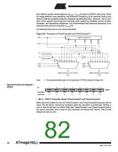
Timer/Counter Interrupt Flag
Register – TIFR
Bit
7
OCF2
R/W
0
6
TOV2
R/W
0
5
4
OCF1A
R/W
0
3
OCF1B
R/W
0
2
TOV1
R/W
0
1
OCF0
R/W
0
0
TOV0
R/W
0
ICF1
R/W
0
TIFR
Read/Write
Initial Value
• Bit 1 – OCF0: Output Compare Flag 0
The OCF0 bit is set (one) when a compare match occurs between the Timer/Counter0
and the data in OCR0 – Output Compare Register0. OCF0 is cleared by hardware when
executing the corresponding interrupt handling vector. Alternatively, OCF0 is cleared by
writing a logic one to the flag. When the I-bit in SREG, OCIE0 (Timer/Counter0 Com-
pare Match Interrupt Enable), and OCF0 are set (one), the Timer/Counter0 Compare
Match Interrupt is executed.
• Bit 0 – TOV0: Timer/Counter0 Overflow Flag
The bit TOV0 is set (one) when an overflow occurs in Timer/Counter0. TOV0 is cleared
by hardware when executing the corresponding interrupt handling vector. Alternatively,
TOV0 is cleared by writing a logic one to the flag. When the SREG I-bit, TOIE0
(Timer/Counter0 Overflow Interrupt Enable), and TOV0 are set (one), the
Timer/Counter0 Overflow interrupt is executed. In phase correct PWM mode, this bit is
set when Timer/Counter0 changes counting direction at $00.
80
ATmega16(L)
2466E–AVR–10/02

 ATMEL [ ATMEL ]