ATmega16(L)
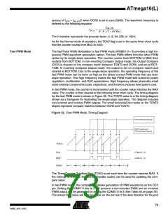
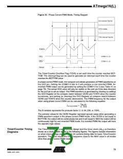
Figure 33. Phase Correct PWM Mode, Timing Diagram
OCn Interrupt Flag Set
OCRn Update
TOVn Interrupt Flag Set
TCNTn
(COMn1:0 = 2)
(COMn1:0 = 3)
OCn
OCn
1
2
3
Period
The Timer/Counter Overflow Flag (TOV0) is set each time the counter reaches BOT-
TOM. The interrupt flag can be used to generate an interrupt each time the counter
reaches the BOTTOM value.
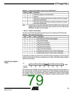
In phase correct PWM mode, the compare unit allows generation of PWM waveforms on
the OC0 pin. Setting the COM01:0 bits to 2 will produce a non-inverted PWM. An
inverted PWM output can be generated by setting the COM01:0 to 3 (see Table 41 on
page 79). The actual OC0 value will only be visible on the port pin if the data direction
for the port pin is set as output. The PWM waveform is generated by clearing (or setting)
the OC0 Register at the compare match between OCR0 and TCNT0 when the counter
increments, and setting (or clearing) the OC0 Register at compare match between
OCR0 and TCNT0 when the counter decrements. The PWM frequency for the output
when using phase correct PWM can be calculated by the following equation:
fclk_I/O
fOCnPCPWM = -----------------
N ⋅ 510
The N variable represents the prescale factor (1, 8, 64, 256, or 1024).
The extreme values for the OCR0 Register represent special cases when generating a
PWM waveform output in the phase correct PWM mode. If the OCR0 is set equal to
BOTTOM, the output will be continuously low and if set equal to MAX the output will be
continuously high for non-inverted PWM mode. For inverted PWM the output will have
the opposite logic values.
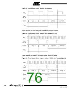
Timer/Counter Timing
Diagrams
The Timer/Counter is a synchronous design and the timer clock (clkT0) is therefore
shown as a clock enable signal in the following figures. The figures include information
on when interrupt flags are set. Figure 34 contains timing data for basic Timer/Counter
operation. The figure shows the count sequence close to the MAX value in all modes
other than phase correct PWM mode.
75
2466E–AVR–10/02

 ATMEL [ ATMEL ]