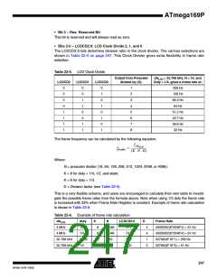
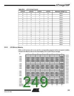
ATmega169P
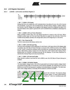
• Bit 0 – LCDBL: LCD Blanking
When this bit is written to one, the display will be blanked after completion of a frame. All seg-
ment and common pins will be driven to ground.
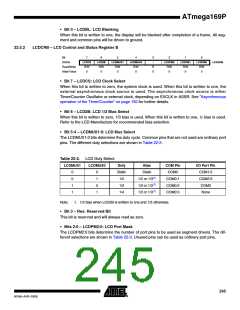
22.5.2
LCDCRB – LCD Control and Status Register B
Bit
7
6
5
4
LCDMUX0
R/W
3
–
2
LCDPM2
R/W
0
1
LCDPM1
R/W
0
0
LCDPM0
R/W
0
LCDCS
LCD2B
LCDMUX1
LCDCRB
(0xE5)
Read/Write
Initial Value
R/W
0
R/W
0
R/W
0
R
0
0
• Bit 7 – LCDCS: LCD Clock Select
When this bit is written to zero, the system clock is used. When this bit is written to one, the
external asynchronous clock source is used. The asynchronous clock source is either
Timer/Counter Oscillator or external clock, depending on EXCLK in ASSR. See ”Asynchronous
operation of the Timer/Counter” on page 150 for further details.
• Bit 6 – LCD2B: LCD 1/2 Bias Select
When this bit is written to zero, 1/3 bias is used. When this bit is written to one, ½ bias is used.
Refer to the LCD Manufacture for recommended bias selection.
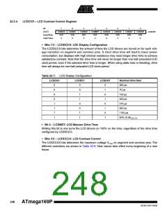
• Bit 5:4 – LCDMUX1:0: LCD Mux Select
The LCDMUX1:0 bits determine the duty cycle. Common pins that are not used are ordinary port
pins. The different duty selections are shown in Table 22-2.
Table 22-2. LCD Duty Select
LCDMUX1
LCDMUX0
Duty
Static
1/2
Bias
COM Pin
COM0
I/O Port Pin
COM1:3
COM2:3
COM3
0
0
1
1
0
1
0
1
Static
1/2 or 1/3(1)
1/2 or 1/3(1)
1/2 or 1/3(1)
COM0:1
COM0:2
COM0:3
1/3
1/4
None
Note:
1. 1/2 bias when LCD2B is written to one and 1/3 otherwise.
• Bit 3 – Res: Reserved Bit
This bit is reserved and will always read as zero.
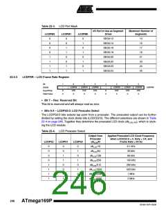
• Bits 2:0 – LCDPM2:0: LCD Port Mask
The LCDPM2:0 bits determine the number of port pins to be used as segment drivers. The dif-
ferent selections are shown in Table 22-3. Unused pins can be used as ordinary port pins.
245
8018A–AVR–03/06

 ATMEL [ ATMEL ]