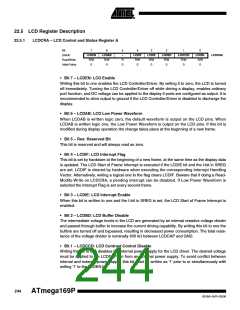
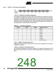
22.5.4
LCDCCR – LCD Contrast Control Register
Bit
7
LCDDC2
R/W
0
6
LCDDC1
R/W
0
5
LCDDC0
R/W
0
4
LCDMDT
R/W
3
LCDCC3
R/W
0
2
LCDCC2
R/W
0
1
LCDCC1
R/W
0
0
LCDCC0
R/W
0
LCDCCR
(0xE7)
Read/Write
Initial Value
0
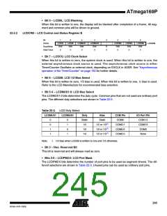
• Bits 7:5 – LCDDC2:0: LDC Display Configuration
The LCDDC2:0 bits determine the amount of time the LCD drivers are turned on for each volt-
age transition on segment and common pins. A short drive time will lead to lower power
consumption, but displays with high internal resistance may need longer drive time to achieve
satisfactory contrast. Note that the drive time will never be longer than one half prescaled LCD
clock period, even if the selected drive time is longer. When using static bias or blanking, drive
time will always be one half prescaled LCD clock period.
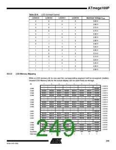
Table 22-7. LCD Display Configuration
LCDDC2
LCDDC1
LCDDC0
Nominal drive time
300 µs
0
0
0
0
1
1
1
1
0
0
1
1
0
0
1
1
0
1
0
1
0
1
0
1
70 µs
150 µs
450 µs
575 µs
850 µs
1150 µs
50ꢀ of clkLCD_PS
• Bit 4 – LCDMDT: LCD Maxium Drive Time
Writing this bit to one turns the LCD drivers on 100ꢀ on the time, regardless of the drive time
configured by LCDDC2:0.
• Bits 3:0 – LCDCC3:0: LCD Contrast Control
The LCDCC3:0 bits determine the maximum voltage VLCD on segment and common pins. The
different selections are shown in Table 22-8. New values take effect every beginning of a new
frame.
248
ATmega169P
8018A–AVR–03/06

 ATMEL [ ATMEL ]