Table 22-3. LCD Port Mask
I/O Port in Use as Segment
Driver
Maximum Number of
Segments
LCDPM2
LCDPM1
LCDPM0
0
0
0
0
1
1
1
1
0
0
1
1
0
0
1
1
0
1
0
1
0
1
0
1
SEG0:12
SEG0:14
SEG0:16
SEG0:18
SEG0:20
SEG0:22
SEG0:23
SEG0:24
13
15
17
19
21
23
24
25
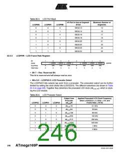
22.5.3
LCDFRR – LCD Frame Rate Register
Bit
7
–
6
LCDPS2
R/W
0
5
LCDPS1
R/W
0
4
LCDPS0
R/W
0
3
–
2
LCDCD2
R/W
0
1
0
LCDCD1
R/W
0
LCDCD0
R/W
0
LCDFRR
(0xE6)
Read/Write
Initial Value
R
0
R
0
• Bit 7 – Res: Reserved Bit
This bit is reserved and will always read as zero.
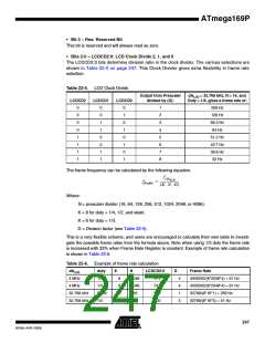
• Bits 6:4 – LCDPS2:0: LCD Prescaler Select
The LCDPS2:0 bits selects tap point from a prescaler. The prescaled output can be further
divided by setting the clock divide bits (LCDCD2:0). The different selections are shown in Table
22-4 on page 246. Together they determine the prescaled LCD clock (clkLCD_PS), which is clock-
ing the LCD module.
Table 22-4. LCD Prescaler Select
Output from
Prescaler
clkLCD/N
Applied Prescaled LCD Clock Frequency
when LCDCD2:0 = 0, Duty = 1/4, and
Frame Rate = 64 Hz
LCDPS2
LCDPS1
LCDPS0
0
0
0
0
1
1
1
1
0
0
1
1
0
0
1
1
0
1
0
1
0
1
0
1
clkLCD/16
clkLCD/64
8.1 kHz
33 kHz
66 kHz
130 kHz
260 kHz
520 kHz
1 MHz
clkLCD/128
clkLCD/256
clkLCD/512
clkLCD/1024
clkLCD/2048
clkLCD/4096
2 MHz
246
ATmega169P
8018A–AVR–03/06

 ATMEL [ ATMEL ]