ATmega640/1280/1281/2560/2561
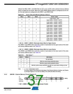
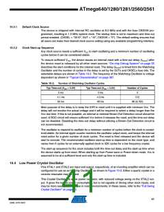
default, the SRL2, SRL1, and SRL0 bits are set to zero and the entire external memory address
space is treated as one sector. When the entire SRAM address space is configured as one sec-
tor, the wait-states are configured by the SRW11 and SRW10 bits.
Figure 9-7. Sector limits with different settings of SRL2:0
SRL2
SRL1
SRL0
Sector Limits
Lower sector = N/A
Upper sector = 0x2200 - 0xFFFF
0
0
x
Lower sector = 0x2200 - 0x3FFF
Upper sector = 0x4000 - 0xFFFF
0
0
1
1
1
1
1
1
0
0
1
1
0
1
0
1
0
1
Lower sector = 0x2200 - 0x5FFF
Upper sector = 0x6000 - 0xFFFF
Lower sector = 0x2200 - 0x7FFF
Upper sector = 0x8000 - 0xFFFF
Lower sector = 0x2200 - 0x9FFF
Upper sector = 0xA000 - 0xFFFF
Lower sector = 0x2200 - 0xBFFF
Upper sector = 0xC000 - 0xFFFF
Lower sector = 0x2200 - 0xDFFF
Upper sector = 0xE000 - 0xFFFF
• Bit 3:2 – SRW11, SRW10: Wait-state Select Bits for Upper Sector
The SRW11 and SRW10 bits control the number of wait-states for the upper sector of the exter-
nal memory address space, see Table 9-2.
• Bit 1:0 – SRW01, SRW00: Wait-state Select Bits for Lower Sector
The SRW01 and SRW00 bits control the number of wait-states for the lower sector of the exter-
nal memory address space, see Table 9-2.
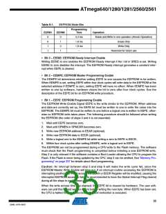
Table 9-2.
Wait States(1)
SRWn0
SRWn1
Wait States
0
0
1
0
1
0
No wait-states
Wait one cycle during read/write strobe
Wait two cycles during read/write strobe
Wait two cycles during read/write and wait one cycle before driving out new
1
1
address
Note:
1. n = 0 or 1 (lower/upper sector).
For further details of the timing and wait-states of the External Memory Interface, see Figures
9-3 through Figures 9-5 for how the setting of the SRW bits affects the timing.
9.4.2
XMCRB – External Memory Control Register B
Bit
7
XMBK
R/W
0
6
–
5
–
4
–
3
–
2
XMM2
R/W
0
1
XMM1
R/W
0
0
XMM0
R/W
0
(0x75)
XMCRB
Read/Write
Initial Value
R
0
R
0
R
0
R
0
• Bit 7– XMBK: External Memory Bus-keeper Enable
37
2549L–AVR–08/07

 ATMEL [ ATMEL ]