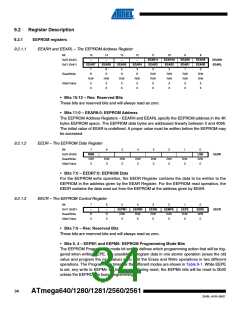
• Bit 0 – EERE: EEPROM Read Enable
The EEPROM Read Enable Signal EERE is the read strobe to the EEPROM. When the correct
address is set up in the EEAR Register, the EERE bit must be written to a logic one to trigger the
EEPROM read. The EEPROM read access takes one instruction, and the requested data is
available immediately. When the EEPROM is read, the CPU is halted for four cycles before the
next instruction is executed.
The user should poll the EEPE bit before starting the read operation. If a write operation is in
progress, it is neither possible to read the EEPROM, nor to change the EEAR Register.
9.3
General Purpose registers
9.3.1
GPIOR2 – General Purpose I/O Register 2
Bit
7
MSB
R/W
0
6
5
4
3
2
1
0
0x2B (0x4B)
Read/Write
Initial Value
LSB
R/W
0
GPIOR2
R/W
R/W
R/W
R/W
R/W
R/W
0
0
0
0
0
0
9.3.2
9.3.3
GPIOR1 – General Purpose I/O Register 1
Bit
7
MSB
R/W
0
6
5
4
3
2
1
0
0x2A (0x4A)
Read/Write
Initial Value
LSB
R/W
0
GPIOR1
R/W
R/W
R/W
R/W
R/W
R/W
0
0
0
0
0
0
GPIOR0 – General Purpose I/O Register 0
Bit
7
MSB
R/W
0
6
5
4
3
2
1
0
0x1E (0x3E)
Read/Write
Initial Value
LSB
R/W
0
GPIOR0
R/W
R/W
R/W
R/W
R/W
R/W
0
0
0
0
0
0
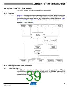
9.4
External Memory registers
9.4.1
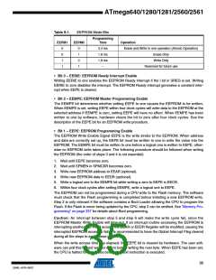
XMCRA – External Memory Control Register A
Bit
7
6
SRL2
R/W
0
5
SRL1
R/W
0
4
SRL0
R/W
0
3
SRW11
R/W
0
2
SRW10
R/W
0
1
SRW01
R/W
0
0
SRW00
R/W
0
“(0x74)”
Read/Write
Initial Value
SRE
R/W
0
XMCRA
• Bit 7 – SRE: External SRAM/XMEM Enable
Writing SRE to one enables the External Memory Interface.The pin functions AD7:0, A15:8,
ALE, WR, and RD are activated as the alternate pin functions. The SRE bit overrides any pin
direction settings in the respective data direction registers. Writing SRE to zero, disables the
External Memory Interface and the normal pin and data direction settings are used.
• Bit 6:4 – SRL2:0: Wait-state Sector Limit
It is possible to configure different wait-states for different External Memory addresses. The
external memory address space can be divided in two sectors that have separate wait-state bits.
The SRL2, SRL1, and SRL0 bits select the split of the sectors, see Table 9-7 and Figure 9-1. By
36
ATmega640/1280/1281/2560/2561
2549L–AVR–08/07

 ATMEL [ ATMEL ]