ATmega640/1280/1281/2560/2561
10.3.1
10.3.2
Default Clock Source
The device is shipped with internal RC oscillator at 8.0 MHz and with the fuse CKDIV8 pro-
grammed, resulting in 1.0 MHz system clock. The startup time is set to maximum and time-out
period enabled. (CKSEL = "0010", SUT = "10", CKDIV8 = "0"). The default setting ensures that
all users can make their desired clock source setting using any available programming interface.
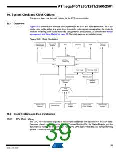
Clock Start-up Sequence
Any clock source needs a sufficient VCC to start oscillating and a minimum number of oscillating
cycles before it can be considered stable.
To ensure sufficient VCC, the device issues an internal reset with a time-out delay (tTOUT) after
the device reset is released by all other reset sources. “On-chip Debug System” on page 55
describes the start conditions for the internal reset. The delay (tTOUT) is timed from the Watchdog
Oscillator and the number of cycles in the delay is set by the SUTx and CKSELx fuse bits. The
selectable delays are shown in Table 10-2. The frequency of the Watchdog Oscillator is voltage
dependent as shown in “Typical Characteristics” on page 387.
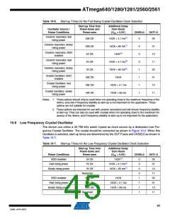
Table 10-2. Number of Watchdog Oscillator Cycles
Typ Time-out (VCC = 5.0V)
Typ Time-out (VCC = 3.0V)
Number of Cycles
0 ms
4.1 ms
65 ms
0 ms
4.3 ms
69 ms
0
512
8K (8,192)
Main purpose of the delay is to keep the AVR in reset until it is supplied with minimum Vcc. The
delay will not monitor the actual voltage and it will be required to select a delay longer than the
Vcc rise time. If this is not possible, an internal or external Brown-Out Detection circuit should be
used. A BOD circuit will ensure sufficient Vcc before it releases the reset, and the time-out delay
can be disabled. Disabling the time-out delay without utilizing a Brown-Out Detection circuit is
not recommended.
The oscillator is required to oscillate for a minimum number of cycles before the clock is consid-
ered stable. An internal ripple counter monitors the oscillator output clock, and keeps the internal
reset active for a given number of clock cycles. The reset is then released and the device will
start to execute. The recommended oscillator start-up time is dependent on the clock type, and
varies from 6 cycles for an externally applied clock to 32K cycles for a low frequency crystal.
The start-up sequence for the clock includes both the time-out delay and the start-up time when
the device starts up from reset. When starting up from Power-save or Power-down mode, Vcc is
assumed to be at a sufficient level and only the start-up time is included.
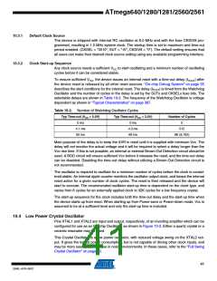
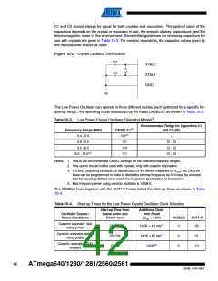
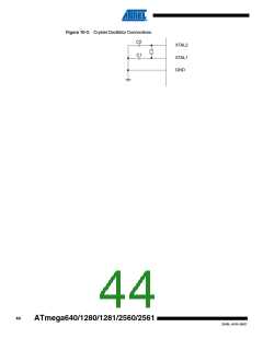
10.4 Low Power Crystal Oscillator
Pins XTAL1 and XTAL2 are input and output, respectively, of an inverting amplifier which can be
configured for use as an On-chip Oscillator, as shown in Figure 10-2. Either a quartz crystal or a
ceramic resonator may be used.
This Crystal Oscillator is a low power oscillator, with reduced voltage swing on the XTAL2 out-
put. It gives the lowest power consumption, but is not capable of driving other clock inputs, and
may be more susceptible to noise in noisy environments. In these cases, refer to the “Full Swing
Crystal Oscillator” on page 43.
41
2549L–AVR–08/07

 ATMEL [ ATMEL ]