ATmega640/1280/1281/2560/2561
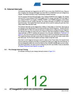
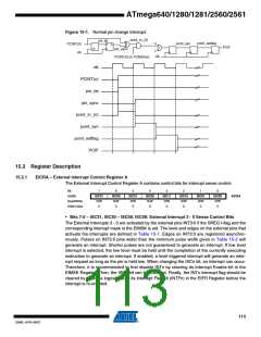
Figure 15-1. Normal pin change interrupt.
pcint_in_(0)
pin_lat
pcint_setflag
0
x
pcint_syn
PCINT(0)
clk
D
Q
PCIF
LE
pin_sync
PCINT(0) in PCMSK(x)
clk
clk
PCINT(n)
pin_lat
pin_sync
pcint_in_(n)
pcint_syn
pcint_setflag
PCIF
15.2 Register Description
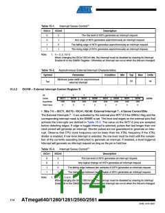
15.2.1
EICRA – External Interrupt Control Register A
The External Interrupt Control Register A contains control bits for interrupt sense control.
Bit
7
ISC31
R/W
0
6
ISC30
R/W
0
5
ISC21
R/W
0
4
ISC20
R/W
0
3
ISC11
R/W
0
2
ISC10
R/W
0
1
ISC01
R/W
0
0
ISC00
R/W
0
(0x69)
EICRA
Read/Write
Initial Value
• Bits 7:0 – ISC31, ISC30 – ISC00, ISC00: External Interrupt 3 - 0 Sense Control Bits
The External Interrupts 3 - 0 are activated by the external pins INT3:0 if the SREG I-flag and the
corresponding interrupt mask in the EIMSK is set. The level and edges on the external pins that
activate the interrupts are defined in Table 15-1. Edges on INT3:0 are registered asynchro-
nously. Pulses on INT3:0 pins wider than the minimum pulse width given in Table 15-2 will
generate an interrupt. Shorter pulses are not guaranteed to generate an interrupt. If low level
interrupt is selected, the low level must be held until the completion of the currently executing
instruction to generate an interrupt. If enabled, a level triggered interrupt will generate an inter-
rupt request as long as the pin is held low. When changing the ISCn bit, an interrupt can occur.
Therefore, it is recommended to first disable INTn by clearing its Interrupt Enable bit in the
EIMSK Register. Then, the ISCn bit can be changed. Finally, the INTn interrupt flag should be
cleared by writing a logical one to its Interrupt Flag bit (INTFn) in the EIFR Register before the
interrupt is re-enabled.
113
2549L–AVR–08/07

 ATMEL [ ATMEL ]