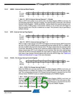
When the PCIE0 bit is set (one) and the I-bit in the Status Register (SREG) is set (one), pin
change interrupt 0 is enabled. Any change on any enabled PCINT7:0 pin will cause an interrupt.
The corresponding interrupt of Pin Change Interrupt Request is executed from the PCI0 Interrupt
Vector. PCINT7:0 pins are enabled individually by the PCMSK0 Register.
15.2.6
PCIFR – Pin Change Interrupt Flag Register
Bit
0x1B (0x3B)
7
6
5
–
4
–
3
–
2
PCIF2
R/W
0
1
PCIF1
R/W
0
0
PCIF0
R/W
0
–
–
PCIFR
Read/Write
R
0
R
0
R
0
R
0
R
0
Initial Value
• Bit 2 – PCIF2: Pin Change Interrupt Flag 1
When a logic change on any PCINT23:16 pin triggers an interrupt request, PCIF2 becomes set
(one). If the I-bit in SREG and the PCIE2 bit in PCICR are set (one), the MCU will jump to the
corresponding Interrupt Vector. The flag is cleared when the interrupt routine is executed. Alter-
natively, the flag can be cleared by writing a logical one to it.
• Bit 1 – PCIF1: Pin Change Interrupt Flag 1
When a logic change on any PCINT15:8 pin triggers an interrupt request, PCIF1 becomes set
(one). If the I-bit in SREG and the PCIE1 bit in PCICR are set (one), the MCU will jump to the
corresponding Interrupt Vector. The flag is cleared when the interrupt routine is executed. Alter-
natively, the flag can be cleared by writing a logical one to it.
• Bit 0 – PCIF0: Pin Change Interrupt Flag 0
When a logic change on any PCINT7:0 pin triggers an interrupt request, PCIF0 becomes set
(one). If the I-bit in SREG and the PCIE0 bit in PCICR are set (one), the MCU will jump to the
corresponding Interrupt Vector. The flag is cleared when the interrupt routine is executed. Alter-
natively, the flag can be cleared by writing a logical one to it.
15.2.7
PCMSK2 – Pin Change Mask Register 2
Bit
7
6
5
PCINT21
R/W
0
4
PCINT20
R/W
0
3
PCINT19
R/W
0
2
PCINT18
R/W
0
1
PCINT17
R/W
0
0
PCINT16
R/W
0
PCINT23
R/W
0
PCINT22
R/W
0
PCMSK2
(0x6D)
Read/Write
Initial Value
• Bit 7:0 – PCINT23:16: Pin Change Enable Mask 23:16
Each PCINT23:16-bit selects whether pin change interrupt is enabled on the corresponding I/O
pin. If PCINT23:16 is set and the PCIE2 bit in PCICR is set, pin change interrupt is enabled on
the corresponding I/O pin. If PCINT23:16 is cleared, pin change interrupt on the corresponding
I/O pin is disabled.
15.2.8
PCMSK1 – Pin Change Mask Register 1
Bit
7
6
5
PCINT13
R/W
0
4
PCINT12
R/W
0
3
PCINT11
R/W
0
2
PCINT10
R/W
0
1
PCINT9
R/W
0
0
PCINT8
R/W
0
PCINT15
R/W
0
PCINT14
R/W
0
PCMSK1
(0x6C)
Read/Write
Initial Value
• Bit 7:0 – PCINT15:8: Pin Change Enable Mask 15:8
Each PCINT15:8-bit selects whether pin change interrupt is enabled on the corresponding I/O
pin. If PCINT15:8 is set and the PCIE1 bit in EIMSK is set, pin change interrupt is enabled on the
116
ATmega640/1280/1281/2560/2561
2549L–AVR–08/07

 ATMEL [ ATMEL ]