AT90PWM2/3/2B/3B
(TXBn = 0) is being transmitted. The slave MCUs must in this case be set to use a 9-bit charac-
ter frame format.
The following procedure should be used to exchange data in Multi-processor Communication
mode:
1. All Slave MCUs are in Multi-processor Communication mode (MPCM in
UCSRA is set).
2. The Master MCU sends an address frame, and all slaves receive and read this frame. In
the Slave MCUs, the RXC flag in UCSRA will be set as normal.
3. Each Slave MCU reads the UDR Register and determines if it has been selected. If so, it
clears the MPCM bit in UCSRA, otherwise it waits for the next address byte and keeps
the MPCM setting.
4. The addressed MCU will receive all data frames until a new address frame is received.
The other Slave MCUs, which still have the MPCM bit set, will ignore the data frames.
5. When the last data frame is received by the addressed MCU, the addressed MCU sets
the MPCM bit and waits for a new address frame from master. The process then repeats
from 2.
Using any of the 5- to 8-bit character frame formats is possible, but impractical since the
Receiver must change between using N and N+1 character frame formats. This makes full-
duplex operation difficult since the Transmitter and Receiver use the same character size set-
ting. If 5- to 8-bit character frames are used, the Transmitter must be set to use two stop bit
(USBS = 1) since the first stop bit is used for indicating the frame type.
18.10 USART Register Description
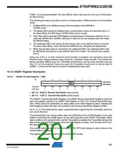
18.10.1 USART I/O Data Register – UDR
Bit
7
6
5
4
3
2
1
0
RXB[7:0]
TXB[7:0]
UDR (Read)
UDR (Write)
Read/Write
Initial Value
R/W
0
R/W
0
R/W
0
R/W
0
R/W
0
R/W
0
R/W
0
R/W
0
• Bit 7:0 – RxB7:0: Receive Data Buffer (read access)
• Bit 7:0 – TxB7:0: Transmit Data Buffer (write access)
The USART Transmit Data Buffer Register and USART Receive Data Buffer Registers share the
same I/O address referred to as USART Data Register or UDR. The Transmit Data Buffer Reg-
ister (TXBn) will be the destination for data written to the UDR Register location. Reading the
UDR Register location will return the contents of the Receive Data Buffer Register (RXBn).
For 5-, 6-, or 7-bit characters the upper unused bits will be ignored by the Transmitter and set to
zero by the Receiver.
The transmit buffer can only be written when the UDRE flag in the UCSRA Register is set. Data
written to UDR when the UDRE flag is not set, will be ignored by the USART Transmitter. When
data is written to the transmit buffer, and the Transmitter is enabled, the Transmitter will load the
data into the Transmit Shift Register when the Shift Register is empty. Then the data will be seri-
ally transmitted on the TxDn pin.
The receive buffer consists of a two level FIFO. The FIFO will change its state whenever the
receive buffer is accessed.
This register is available in both USART and EUSART modes.
201
4317J–AVR–08/10

 ATMEL [ ATMEL ]