AT90PWM2/3/2B/3B
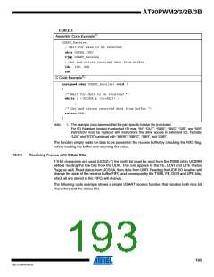
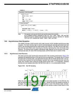
TABLE 2.
Assembly Code Example(1)
USART_Flush:
sbis UCSRA, RXC0
ret
lds r16, UDR
rjmp USART_Flush
C Code Example(1)
void USART_Flush( void )
{
unsigned char dummy;
while ( UCSRA & (1<<RXC0) ) dummy = UDR;
}
Note:
1. The example code assumes that the part specific header file is included.
For I/O Registers located in extended I/O map, “IN”, “OUT”, “SBIS”, “SBIC”, “CBI”, and “SBI”
instructions must be replaced with instructions that allow access to extended I/O. Typically
“LDS” and “STS” combined with “SBRS”, “SBRC”, “SBR”, and “CBR”.
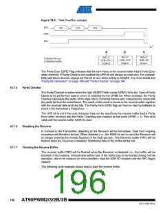
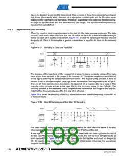
18.8 Asynchronous Data Reception
The USART includes a clock recovery and a data recovery unit for handling asynchronous data
reception. The clock recovery logic is used for synchronizing the internally generated baud rate
clock to the incoming asynchronous serial frames at the RxD pin. The data recovery logic sam-
ples and low pass filters each incoming bit, thereby improving the noise immunity of the
Receiver. The asynchronous reception operational range depends on the accuracy of the inter-
nal baud rate clock, the rate of the incoming frames, and the frame size in number of bits.
18.8.1
Asynchronous Clock Recovery
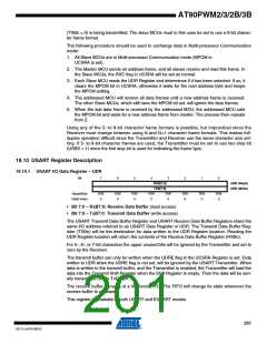
The clock recovery logic synchronizes internal clock to the incoming serial frames. Figure 18-6
illustrates the sampling process of the start bit of an incoming frame. The sample rate is 16 times
the baud rate for Normal mode, and eight times the baud rate for Double Speed mode. The hor-
izontal arrows illustrate the synchronization variation due to the sampling process. Note the
larger time variation when using the Double Speed mode (U2X = 1) of operation. Samples
denoted zero are samples done when the RxD line is idle (i.e., no communication activity).
Figure 18-6. Start Bit Sampling
RxDn
IDLE
START
BIT 0
Sample
(U2Xn = 0)
0
0
1
1
2
3
2
4
5
3
6
7
4
8
9
5
10
11
6
12
13
7
14
15
8
16
1
1
2
3
Sample
(U2Xn = 1)
0
2
When the clock recovery logic detects a high (idle) to low (start) transition on the RxD line, the
start bit detection sequence is initiated. Let sample 1 denote the first zero-sample as shown in
the figure. The clock recovery logic then uses samples 8, 9, and 10 for Normal mode, and sam-
ples 4, 5, and 6 for Double Speed mode (indicated with sample numbers inside boxes on the
197
4317J–AVR–08/10

 ATMEL [ ATMEL ]