AT90PWM2/3/2B/3B
Note that fclkio depends on the stability of the system clock source. It is therefore recommended
to add some margin to avoid possible loss of data due to frequency variations.
18.3.4
Synchronous Clock Operation
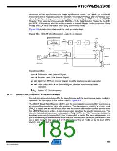
When synchronous mode is used (UMSEL = 1), the XCK pin will be used as either clock input
(Slave) or clock output (Master). The dependency between the clock edges and data sampling
or data change is the same. The basic principle is that data input (on RxD) is sampled at the
opposite XCK clock edge of the edge the data output (TxDn) is changed.
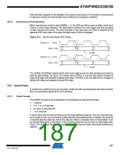
Figure 18-3. Synchronous Mode XCK Timing.
UCPOLn = 1
XCKn
RxDn / TxDn
Sample
Sample
UCPOLn = 0
XCKn
RxDn / TxDn
The UCPOL bit UCRSnC selects which XCK clock edge is used for data sampling and which is
used for data change. As Figure 18-3 shows, when UCPOL is zero the data will be changed at
rising XCK edge and sampled at falling XCK edge. If UCPOL is set, the data will be changed at
falling XCK edge and sampled at rising XCK edge.
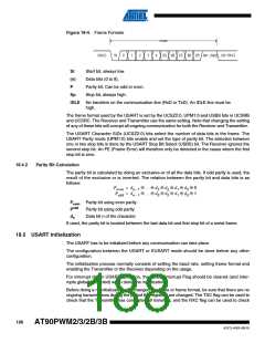
18.4 Serial Frame
A serial frame is defined to be one character of data bits with synchronization bits (start and stop
bits), and optionally a parity bit for error checking.
18.4.1
Frame Formats
The USART accepts all 30 combinations of the following as valid frame formats:
•
1 start bit
•
•
•
5, 6, 7, 8, or 9 data bits
no, even or odd parity bit
1 or 2 stop bits
A frame starts with the start bit followed by the least significant data bit. Then the next data bits,
up to a total of nine, are succeeding, ending with the most significant bit. If enabled, the parity bit
is inserted after the data bits, before the stop bits. When a complete frame is transmitted, it can
be directly followed by a new frame, or the communication line can be set to an idle (high) state.
Figure 18-4 illustrates the possible combinations of the frame formats. Bits inside brackets are
optional.
187
4317J–AVR–08/10

 ATMEL [ ATMEL ]