AT90PWM2/3/2B/3B
chronous, Master synchronous and Slave synchronous mode. The UMSEL bit in USART
Control and Status Register C (UCSRC) selects between asynchronous and synchronous oper-
ation. Double Speed (asynchronous mode only) is controlled by the U2X found in the UCSRA
Register. When using synchronous mode (UMSEL = 1), the Data Direction Register for the XCK
pin (DDR_XCK) controls whether the clock source is internal (Master mode) or external (Slave
mode). The XCK pin is only active when using synchronous mode.
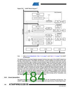
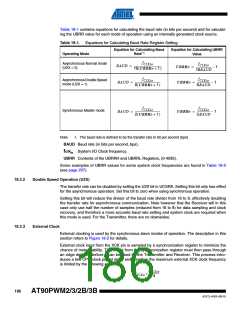
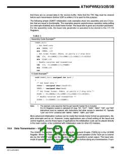
Figure 18-2 shows a block diagram of the clock generation logic.
Figure 18-2. USART Clock Generation Logic, Block Diagram
UBRRn
U2Xn
f
clkio
UBRRn+1
Prescaling
Down-Counter
/2
/4
/2
0
1
0
1
clkio
txn clk
UMSELn
rxn clk
DDR_XCKn
Sync
Register
Edge
Detector
0
1
xn cki
XCKn
Pin
xn cko
DDR_XCKn
UCPOLn
1
0
Signal description:
txn clk Transmitter clock (Internal Signal).
rxn clk Receiver base clock (Internal Signal).
xn cki Input from XCK pin (internal Signal). Used for synchronous slave operation.
xn cko Clock output to XCK pin (Internal Signal). Used for synchronous master
operation.
fclkio System I/O Clock frequency.
18.3.1
Internal Clock Generation – Baud Rate Generator
Internal clock generation is used for the asynchronous and the synchronous master modes of
operation. The description in this section refers to Figure 18-2.
The USART Baud Rate Register (UBRR) and the down-counter connected to it function as a
programmable prescaler or baud rate generator. The down-counter, running at system clock
(fclkio), is loaded with the UBRR value each time the counter has counted down to zero or when
the UBRRL Register is written. A clock is generated each time the counter reaches zero. This
clock is the baud rate generator clock output (= fclkio/(UBRR+1)). The Transmitter divides the
baud rate generator clock output by 2, 8 or 16 depending on mode. The baud rate generator out-
put is used directly by the Receiver’s clock and data recovery units. However, the recovery units
use a state machine that uses 2, 8 or 16 states depending on mode set by the state of the
UMSEL, U2X and DDR_XCK bits.
185
4317J–AVR–08/10

 ATMEL [ ATMEL ]