PDF
最近搜索
热门搜索
发布采购

| 型号: | AT77C105A |
| PDF下载: | 下载PDF文件 查看货源 |
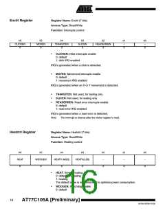
| 内容描述: | 的FingerChip热指纹扫描传感器,基于硬件的导航和点击功能,扩展I / O范围( 1.8-3.3V ) [FingerChip Thermal Fingerprint Sweep Sensor, Hardware Based Navigation and Click Functions, Extended I/O range(1.8-3.3V)] |
| 分类和应用: | 传感器 |
| 文件页数/大小: | 39 页 / 451 K |
| 品牌: |  ATMEL [ ATMEL ] ATMEL [ ATMEL ] |
专业IC领域供求交易平台:提供全面的IC Datasheet资料和资讯,Datasheet 1000万数据,IC品牌1000多家。