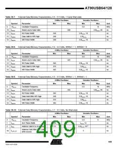
AT90USB64/128
30.7 SPI Timing Characteristics
See Figure 30-4 and Figure 30-5 for details.
Table 30-3. SPI Timing Parameters
Description
SCK period
SCK high/low
Rise/Fall time
Setup
Mode
Master
Master
Master
Master
Master
Master
Master
Master
Slave
Min
Typ
Max
1
2
See Table 17-4
50% duty cycle
3
TBD
10
4
5
Hold
10
6
Out to SCK
SCK to out
SCK to out high
SS low to out
SCK period
SCK high/low(1)
Rise/Fall time
Setup
0.5 • tsck
10
7
8
10
9
15
ns
10
11
12
13
14
15
16
17
18
Slave
4 • tck
2 • tck
Slave
Slave
Slave
Slave
Slave
Slave
Slave
Slave
TBD
10
tck
Hold
SCK to out
SCK to SS high
SS high to tri-state
SS low to SCK
15
10
20
20
Note:
1. In SPI Programming mode the minimum SCK high/low period is:
- 2 tCLCL for fCK < 12 MHz
- 3 tCLCL for fCK > 12 MHz
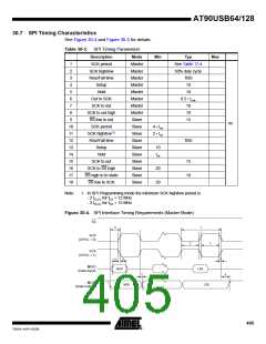
Figure 30-4. SPI Interface Timing Requirements (Master Mode)
SS
6
1
SCK
(CPOL = 0)
2
2
SCK
(CPOL = 1)
4
5
3
MISO
(Data Input)
MSB
...
LSB
7
8
MOSI
(Data Output)
MSB
...
LSB
405
7593A–AVR–02/06

 ATMEL [ ATMEL ]