AT90USB64/128
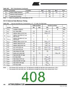
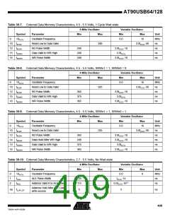
Table 30-7. External Data Memory Characteristics, 4.5 - 5.5 Volts, 1 Cycle Wait-state
8 MHz Oscillator
Variable Oscillator
Symbol
Parameter
Min
Max
Min
Max
16
Unit
MHz
ns
0
1/tCLCL
Oscillator Frequency
Read Low to Data Valid
RD Pulse Width
0.0
10 tRLDV
12 tRLRH
15 tDVWH
16 tWLWH
200
2.0tCLCL-50
240
240
240
2.0tCLCL-10
2.0tCLCL
ns
Data Valid to WR High
WR Pulse Width
ns
2.0tCLCL-10
ns
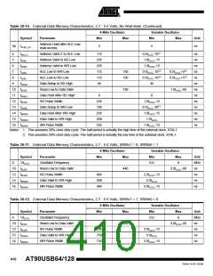
Table 30-8. External Data Memory Characteristics, 4.5 - 5.5 Volts, SRWn1 = 1, SRWn0 = 0
4 MHz Oscillator Variable Oscillator
Symbol
Parameter
Min
Max
Min
Max
16
Unit
MHz
ns
0
1/tCLCL
Oscillator Frequency
Read Low to Data Valid
RD Pulse Width
0.0
10 tRLDV
12 tRLRH
15 tDVWH
16 tWLWH
325
3.0tCLCL-50
365
375
365
3.0tCLCL-10
3.0tCLCL
ns
Data Valid to WR High
WR Pulse Width
ns
3.0tCLCL-10
ns
Table 30-9. External Data Memory Characteristics, 4.5 - 5.5 Volts, SRWn1 = 1, SRWn0 = 1
4 MHz Oscillator Variable Oscillator
Symbol
Parameter
Min
Max
Min
Max
16
Unit
MHz
ns
0
1/tCLCL
Oscillator Frequency
Read Low to Data Valid
RD Pulse Width
0.0
10 tRLDV
12 tRLRH
14 tWHDX
15 tDVWH
16 tWLWH
325
3.0tCLCL-50
365
240
375
365
3.0tCLCL-10
2.0tCLCL-10
3.0tCLCL
ns
Data Hold After WR High
Data Valid to WR High
WR Pulse Width
ns
ns
3.0tCLCL-10
ns
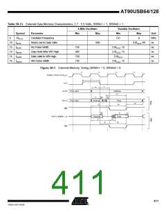
Table 30-10. External Data Memory Characteristics, 2.7 - 5.5 Volts, No Wait-state
4 MHz Oscillator
Variable Oscillator
Symbol
1/tCLCL
tLHLL
Parameter
Min
Max
Min
0.0
Max
Unit
MHz
ns
0
1
2
Oscillator Frequency
ALE Pulse Width
8
235
115
tCLCL-15
0.5tCLCL-10(1)
tAVLL
Address Valid A to ALE Low
ns
Address Hold After ALE Low,
write access
3a tLLAX_ST
5
5
ns
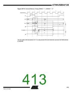
409
7593A–AVR–02/06

 ATMEL [ ATMEL ]