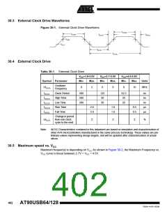
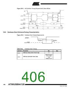
30.3 External Clock Drive Waveforms
Figure 30-1. External Clock Drive Waveforms
VIH1
VIL1
30.4 External Clock Drive
Table 30-1. External Clock Drive
VCC=1.8-5.5V
VCC=2.7-5.5V
VCC=4.5-5.5V
Symbol Parameter
Min.
Max.
Min.
Max.
Min.
Max.
Units
Oscillator
1/tCLCL
0
2
0
8
0
16
MHz
Frequency
tCLCL
tCHCX
tCLCX
tCLCH
tCHCL
Clock Period
High Time
Low Time
Rise Time
Fall Time
500
200
200
125
50
62.5
25
ns
ns
ns
μs
μs
50
25
2.0
2.0
1.6
1.6
0.5
0.5
Change in period
from one clock
cycle to the next
ΔtCLCL
2
2
2
%
Note:
All DC Characteristics contained in this datasheet are based on simulation and characterization of
other AVR microcontrollers manufactured in the same process technology. These values are pre-
liminary values representing design targets, and will be updated after characterization of actual
silicon.
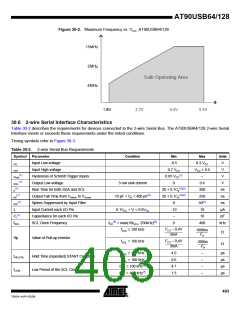
30.5 Maximum speed vs. VCC
Maximum frequency is depending on VCC. As shown in Figure 30-2, the Maximum Frequency vs.
V
CC curve is linear between 2.7V < VCC < 4.5V.
402
AT90USB64/128
7593A–AVR–02/06

 ATMEL [ ATMEL ]