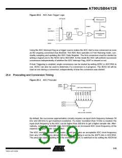
in ADCSRA. The prescaler keeps running for as long as the ADEN bit is set, and is continuously
reset when ADEN is low.
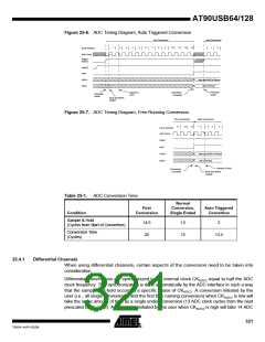
When initiating a single ended conversion by setting the ADSC bit in ADCSRA, the conversion
starts at the following rising edge of the ADC clock cycle. See “Differential Channels” on page
321 for details on differential conversion timing.
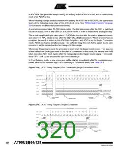
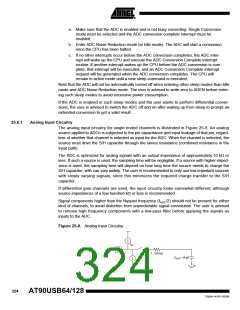
A normal conversion takes 13 ADC clock cycles. The first conversion after the ADC is switched
on (ADEN in ADCSRA is set) takes 25 ADC clock cycles in order to initialize the analog circuitry.
The actual sample-and-hold takes place 1.5 ADC clock cycles after the start of a normal conver-
sion and 13.5 ADC clock cycles after the start of an first conversion. When a conversion is
complete, the result is written to the ADC Data Registers, and ADIF is set. In Single Conversion
mode, ADSC is cleared simultaneously. The software may then set ADSC again, and a new
conversion will be initiated on the first rising ADC clock edge.
When Auto Triggering is used, the prescaler is reset when the trigger event occurs. This assures
a fixed delay from the trigger event to the start of conversion. In this mode, the sample-and-hold
takes place two ADC clock cycles after the rising edge on the trigger source signal. Three addi-
tional CPU clock cycles are used for synchronization logic.
In Free Running mode, a new conversion will be started immediately after the conversion com-
pletes, while ADSC remains high. For a summary of conversion times, see Table 25-1.
Figure 25-4. ADC Timing Diagram, First Conversion (Single Conversion Mode)
Next
First Conversion
Conversion
Cycle Number
1
2
12
13
14
15
16
17
18
19
20
21
22
23
24
25
1
2
3
ADC Clock
ADEN
ADSC
ADIF
Sign and MSB of Result
ADCH
ADCL
LSB of Result
MUX
MUX and REFS
Update
Conversion
Complete
and REFS
Update
Sample & Hold
Figure 25-5. ADC Timing Diagram, Single Conversion
One Conversion
Next Conversion
1
2
3
4
5
6
7
8
9
10
11
12
13
1
2
3
Cycle Number
ADC Clock
ADSC
ADIF
ADCH
Sign and MSB of Result
LSB of Result
ADCL
Sample & Hold
Conversion
Complete
MUX and REFS
Update
MUX and REFS
Update
320
AT90USB64/128
7593A–AVR–02/06

 ATMEL [ ATMEL ]