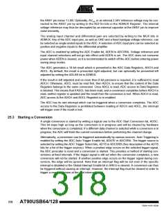
the AREF pin minus 1 LSB. Optionally, AVCC or an internal 2.56V reference voltage may be con-
nected to the AREF pin by writing to the REFSn bits in the ADMUX Register. The internal
voltage reference may thus be decoupled by an external capacitor at the AREF pin to improve
noise immunity.
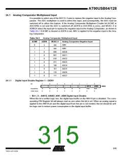
The analog input channel and differential gain are selected by writing to the MUX bits in
ADMUX. Any of the ADC input pins, as well as GND and a fixed bandgap voltage reference, can
be selected as single ended inputs to the ADC. A selection of ADC input pins can be selected as
positive and negative inputs to the differential amplifier.
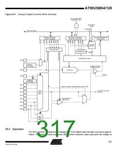
The ADC is enabled by setting the ADC Enable bit, ADEN in ADCSRA. Voltage reference and
input channel selections will not go into effect until ADEN is set. The ADC does not consume
power when ADEN is cleared, so it is recommended to switch off the ADC before entering power
saving sleep modes.
The ADC generates a 10-bit result which is presented in the ADC Data Registers, ADCH and
ADCL. By default, the result is presented right adjusted, but can optionally be presented left
adjusted by setting the ADLAR bit in ADMUX.
If the result is left adjusted and no more than 8-bit precision is required, it is sufficient to read
ADCH. Otherwise, ADCL must be read first, then ADCH, to ensure that the content of the Data
Registers belongs to the same conversion. Once ADCL is read, ADC access to Data Registers
is blocked. This means that if ADCL has been read, and a conversion completes before ADCH is
read, neither register is updated and the result from the conversion is lost. When ADCH is read,
ADC access to the ADCH and ADCL Registers is re-enabled.
The ADC has its own interrupt which can be triggered when a conversion completes. The ADC
access to the Data Registers is prohibited between reading of ADCH and ADCL, the interrupt
will trigger even if the result is lost.
25.3 Starting a Conversion
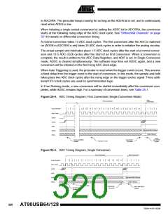
A single conversion is started by writing a logical one to the ADC Start Conversion bit, ADSC.
This bit stays high as long as the conversion is in progress and will be cleared by hardware
when the conversion is completed. If a different data channel is selected while a conversion is in
progress, the ADC will finish the current conversion before performing the channel change.
Alternatively, a conversion can be triggered automatically by various sources. Auto Triggering is
enabled by setting the ADC Auto Trigger Enable bit, ADATE in ADCSRA. The trigger source is
selected by setting the ADC Trigger Select bits, ADTS in ADCSRB (See description of the ADTS
bits for a list of the trigger sources). When a positive edge occurs on the selected trigger signal,
the ADC prescaler is reset and a conversion is started. This provides a method of starting con-
versions at fixed intervals. If the trigger signal is still set when the conversion completes, a new
conversion will not be started. If another positive edge occurs on the trigger signal during con-
version, the edge will be ignored. Note that an interrupt flag will be set even if the specific
interrupt is disabled or the Global Interrupt Enable bit in SREG is cleared. A conversion can thus
be triggered without causing an interrupt. However, the interrupt flag must be cleared in order to
trigger a new conversion at the next interrupt event.
318
AT90USB64/128
7593A–AVR–02/06

 ATMEL [ ATMEL ]