AT90USB64/128
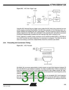
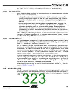
Figure 25-2. ADC Auto Trigger Logic
ADTS[2:0]
PRESCALER
CLKADC
START
ADATE
ADIF
SOURCE 1
.
.
.
.
CONVERSION
LOGIC
EDGE
DETECTOR
SOURCE n
ADSC
Using the ADC Interrupt Flag as a trigger source makes the ADC start a new conversion as soon
as the ongoing conversion has finished. The ADC then operates in Free Running mode, con-
stantly sampling and updating the ADC Data Register. The first conversion must be started by
writing a logical one to the ADSC bit in ADCSRA. In this mode the ADC will perform successive
conversions independently of whether the ADC Interrupt Flag, ADIF is cleared or not.
If Auto Triggering is enabled, single conversions can be started by writing ADSC in ADCSRA to
one. ADSC can also be used to determine if a conversion is in progress. The ADSC bit will be
read as one during a conversion, independently of how the conversion was started.
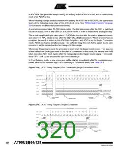
25.4 Prescaling and Conversion Timing
Figure 25-3. ADC Prescaler
ADEN
START
Reset
7-BIT ADC PRESCALER
CK
ADPS0
ADPS1
ADPS2
ADC CLOCK SOURCE
By default, the successive approximation circuitry requires an input clock frequency between 50
kHz and 200 kHz to get maximum resolution. If a lower resolution than 10 bits is needed, the
input clock frequency to the ADC can be higher than 200 kHz to get a higher sample rate. Alter-
natively, setting the ADHSM bit in ADCSRB allows an increased ADC clock frequency at the
expense of higher power consumption.
The ADC module contains a prescaler, which generates an acceptable ADC clock frequency
from any CPU frequency above 100 kHz. The prescaling is set by the ADPS bits in ADCSRA.
The prescaler starts counting from the moment the ADC is switched on by setting the ADEN bit
319
7593A–AVR–02/06

 ATMEL [ ATMEL ]