AT90USB64/128
The settling time and gain stage bandwidth is independent of the ADHSM bit setting.
25.5.1
ADC Input Channels
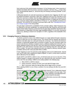
When changing channel selections, the user should observe the following guidelines to ensure
that the correct channel is selected:
• In Single Conversion mode, always select the channel before starting the conversion. The
channel selection may be changed one ADC clock cycle after writing one to ADSC. However,
the simplest method is to wait for the conversion to complete before changing the channel
selection.
• In Free Running mode, always select the channel before starting the first conversion. The
channel selection may be changed one ADC clock cycle after writing one to ADSC. However,
the simplest method is to wait for the first conversion to complete, and then change the
channel selection. Since the next conversion has already started automatically, the next
result will reflect the previous channel selection. Subsequent conversions will reflect the new
channel selection.
When switching to a differential gain channel, the first conversion result may have a poor accu-
racy due to the required settling time for the automatic offset cancellation circuitry. The user
should preferably disregard the first conversion result.
25.5.2
ADC Voltage Reference
The reference voltage for the ADC (VREF) indicates the conversion range for the ADC. Single
ended channels that exceed VREF will result in codes close to 0x3FF. VREF can be selected as
either AVCC, internal 2.56V reference, or external AREF pin.
AVCC is connected to the ADC through a passive switch. The internal 2.56V reference is gener-
ated from the internal bandgap reference (VBG) through an internal amplifier. In either case, the
external AREF pin is directly connected to the ADC, and the reference voltage can be made
more immune to noise by connecting a capacitor between the AREF pin and ground. VREF can
also be measured at the AREF pin with a high impedant voltmeter. Note that VREF is a high
impedant source, and only a capacitive load should be connected in a system.
If the user has a fixed voltage source connected to the AREF pin, the user may not use the other
reference voltage options in the application, as they will be shorted to the external voltage. If no
external voltage is applied to the AREF pin, the user may switch between AVCC and 2.56V as
reference selection. The first ADC conversion result after switching reference voltage source
may be inaccurate, and the user is advised to discard this result.
If differential channels are used, the selected reference should not be closer to AVCC than indi-
cated in Table 30-5 on page 407.
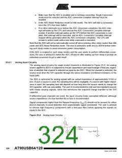
25.6 ADC Noise Canceler
The ADC features a noise canceler that enables conversion during sleep mode to reduce noise
induced from the CPU core and other I/O peripherals. The noise canceler can be used with ADC
Noise Reduction and Idle mode. To make use of this feature, the following procedure should be
used:
323
7593A–AVR–02/06

 ATMEL [ ATMEL ]