Electrical Characteristics
Absolute Maximum Rating
*NOTICE:
Stressing the device beyond the “Absolute Maxi-
mum Ratings” may cause permanent damage.
These are stress ratings only. Operation beyond
the “operating conditions” is not recommended
and extended exposure beyond the “Operating
Conditions” may affect device reliability.
Storage Temperature ......................................... -65 to +150°C
Voltage on any other Pin to VSS .................................... -0.3 to +4.0 V
IOL per I/O Pin ................................................................. 5 mA
Power Dissipation............................................................. 1 W
Operating Conditions
Ambient Temperature Under Bias........................ -40 to +85°C
VDD ................................................................................................................... TBD V
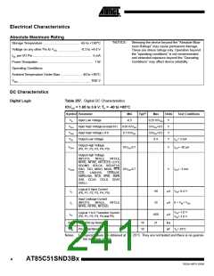
DC Characteristics
Digital Logic
Table 257. Digital DC Characteristics
IOVDD = 1.65 to 3.6 V; TA = -40 to +85°C
Symbol Parameter
Min
Typ(1)
Max
Units
Test Conditions
VIL
Input Low Voltage
-0.5
0.25·IOVDD
IOVDD+0.5
IOVDD+0.5
0.4
V
V
V
V
VIH1
VIH2
VOL
Input High Voltage (except X1)
Input High Voltage ( X1)
Output Low Voltage
0.65·IOVDD
0.7·IOVDD
IOL= 3 mA
IOH= -30 µA
Output High Voltage
(P0, P1, P2, P3, P4, P5)
VOH1
IOVDD-0.7
V
Output High Voltage
(NFD7:0,
NFALE,
NFCLE,
NFRE, NFWE, NFCE3:0, LD7:0,
SDCMD, SDLCK, SDDAT3:0,
VOH2 RXD, TXD, MISO, MOSI, RTS, IOVDD-0.7
LCS, LA0/LRS, LRD/LDE,
V
IOH= -3 mA
LWR/LRW, SCS, SRD, SWR,
SA0, OCLK, DCLK, DDAT,
DSEL)
Logical 0 Input Current
(P0, P1, P2, P3, P4, P5)
IIL
-50
10
μA VIN= 0.4 V
Input Leakage Current
ILI
(NFD7:0,
NFALE,
NFCLE,
μA 0 < VIN< VDD
NFRE, NFWE, NFCE0)
VIN= 1.0 V
μA
Logical 1 to 0 Transition Current
(P0, P1, P2, P3, P4 and P5)
ITL
-650
21
VIN= 2.0 V
RRST RST Pull-Up Resistor
CIO Pin Capacitance
10
16
10
kΩ
pF TA= 25°C
Notes: 1. Typical values are obtained at TA= 25°C. They are not tested and there is no guaran-
tee on these values.
4
AT85C51SND3Bx
7632A–MP3–03/06

 ATMEL [ ATMEL ]