AT85C51SND3Bx
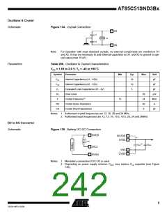
Oscillator & Crystal
Schematic
Figure 134. Crystal Connection
X1
X2
C1
C2
Q
APVSS
Note:
For operation with most standard crystals, no external components are needed on X1
and X2. It may be necessary to add external capacitors on X1 and X2 to ground in spe-
cial cases (max 10 pF).
Parameters
Table 258. Oscillator & Crystal Characteristics
VDD = 1.65 to 3.6 V; TA = -40 to +85°C
Symbol
CX1
CX2
CL
Parameter
Min
Typ
10
10
5
Max
Unit
pF
Internal Capacitance (X1 - VSS)
Internal Capacitance (X2 - VSS)
Equivalent Load Capacitance (X1 - X2)
Drive Level
pF
pF
DL
50
24
40
6
μW
MHz
Ω
F
Crystal Frequency(1)
12
RS
Crystal Series Resistance
Crystal Shunt Capacitance
CS
pF
Notes: 1. Authorized crystal frequencies are 12, 16, 20 and 24 MHz
2. Authorised input frequencies are 12, 13, 16, 19.2, 19.5, 20, 24 and 26MHz
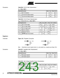
DC to DC Convertor
Schematic
Figure 135. Battery DC-DC Connection
BVDD
RLVDD
(1)
LVDD
LDC
(2)
CDC1
CDC2
DCLI
VSS
CVSS
BVSS
Notes: 1. Mandatory connection if DC-DC is used.
2. Depending on power supply scheme, CDC1 may replace CLV capacitor (see Figure
136).
5
7632A–MP3–03/06

 ATMEL [ ATMEL ]