Parameters
Table 259. DC-DC Filter Characteristics
TA = -40 to +85°C
Symbol Parameter
Min
Typ
10
Max Unit
LDC
DC-DC Inductance
µH
µF
nF
CDC1
CDC2
Low ESR Decoupling Capacitor
Low ESR Decoupling Capacitor
20
100
Table 260. DC-DC Power Characteristics
VBAT = 0.9 to 3.6 V; TA = -40 to +85°C
Symbol Parameter
Min
0.9
1.6
Typ
Max Unit Test Conditions
VBAT
VDC
DC-DC Input Voltage
DC-DC Output Voltage
DC-DC Output Current
Maximum Efficiency
3.6
1.9
40
V
V
IDC = 40 mA
IDC = 40 mA
1.75
IDC
mA VBAT = 1.0 V
HMAX
92
%
VBAT = 1.5 V
FSWITCH Switching Frequency
0.5
1.5
30
3
MHz
KΩ
RDCP
DCPWR Input Pull-Up Resistor
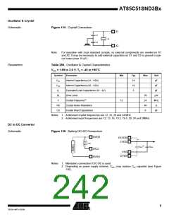
Regulators
Schematic
Figure 136. Regulator Connection
HVDD
RLVDD
VSS
( )
CHV
CLV *
VSS
Note:
Depending on power supply scheme, CLV may replace CDC1 capacitor (see Figure 135).
Parameters
Table 261. Regulator Filter Characteristics
TA = -40 to +85°C
Symbol Parameter
Min
Typ
10
Max Unit
CHV
CLV
Decoupling Capacitor
Decoupling Capacitor
µF
µF
20
Table 262. High Voltage Regulator Power Characteristics
UVCC = 4.4 to 5.5 V; TA = -40 to +85°C
Symbol Parameter
VHV High Voltage Regulator Output Voltage
IHV High Voltage Regulator Output Current
Min
Typ
Max Unit Test Conditions
3.1
3.3
3.5
50
V
IDC = 50 mA
mA
6
AT85C51SND3Bx
7632A–MP3–03/06

 ATMEL [ ATMEL ]