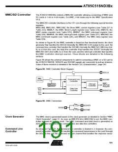
tion from the card through the SDCMD line. These channels are detailed in the following
sections.
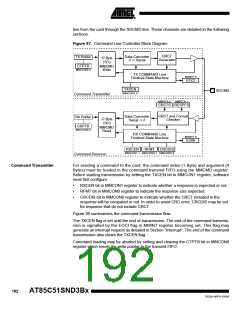
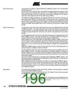
Figure 87. Command Line Controller Block Diagram
CRC7
Generator
Data Converter
// -> Serial
TX Pointer
17-Byte
FIFO
CTPTR
MMCON0.4
MMCMD
Write
TX COMMAND Line
Finished State Machine
MMINT.5
EOCI
TXCEN
MMCON1.0
SDCMD
Command Transmitter
MMSTA.2
MMSTA.1
CRC7S RESPFS
CRC7 and Format
Checker
Data Converter
Serial -> //
RX Pointer
17-Byte
FIFO
MMCMD
CRPTR
MMCON0.5
Read
RX COMMAND Line
Finished State Machine
MMINT.6
EORI
RXCEN
RFMT CRCDIS
MMCON1.1 MMCON0.1 MMCON0.0
Command Receiver
Command Transmitter
For sending a command to the card, the command index (1 Byte) and argument (4
Bytes) must be loaded in the command transmit FIFO using the MMCMD register.
Before starting transmission by setting the TXCEN bit in MMCON1 register, software
must first configure:
•
•
•
RXCEN bit in MMCON1 register to indicate whether a response is expected or not.
RFMT bit in MMCON0 register to indicate the response size expected.
CRCDIS bit in MMCON0 register to indicate whether the CRC7 included in the
response will be computed or not. In order to avoid CRC error, CRCDIS may be set
for response that do not include CRC7.
Figure 88 summarizes the command transmission flow.
The TXCEN flag is set until the end of transmission. The end of the command transmis-
sion is signalled by the EOCI flag in MMINT register becoming set. This flag may
generate an interrupt request as detailed in Section “Interrupt”. The end of the command
transmission also clears the TXCEN flag.
Command loading may be aborted by setting and clearing the CTPTR bit in MMCON0
register which resets the write pointer to the transmit FIFO.
192
AT85C51SND3Bx
7632A–MP3–03/06

 ATMEL [ ATMEL ]