AT85C51SND3Bx
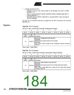
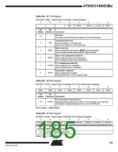
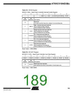
Table 204. NFCON Register
NFCON (1.9Bh) – Nand Flash Controller Control Register
7
6
5
4
3
2
1
0
-
-
-
TRS
NFWP
SPZEN
ECCEN
NFEN
Bit
Bit
Number
Mnemonic Description
Reserved
7-5
4
-
The value read from these bits is always 0. Do not set these bits.
Timing Read Select Bit
TRS
Set to use timing [1; 1] for read cycle.
Clear to use timing [1.5; 0.5] for read cycle.
Write Protect Bit
3
2
1
0
NFWP
SPZEN
ECCEN
NFEN
Set to unprotect the flash devices (NFWP signal de-asserted).
Clear to protect the flash devices (NFWP signal asserted).
Spare Zone management enable Bit
Set to enable the spare zone management
Clear to disable the spare zone management.
ECC management enable Bit
Set to enable the ECC calculation.
Clear to disable the ECC calculation.
General NFC Enable Bit
Set to enable the NF controller.
Clear to put the NFC is in the ‘suspend’ state.
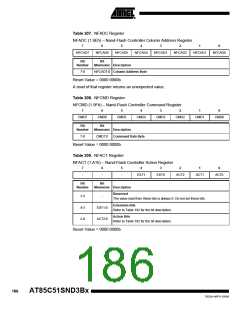
Table 205. NFERR Register
NFERR (1.9Ch) – Nand Flash Controller ECC Error Information Register
7
6
5
4
3
2
1
0
ERR7
ERR6
ERR5
ERR4
ERR3
ERR2
ERR1
ERR0
Bit
Bit
Number
Mnemonic Description
Error Descriptor 4-byte Data FIFO
7-0
ERR7:0
Sequential reading returns the 4-byte ECC error descriptor (see Table 199).
This register is updated following an ECC error (ECCERRI set).
Reset Value = 0000 0000b
Table 206. NFADR Register
NFADR (1.9Dh) – Nand Flash Controller Row Address Register
7
6
5
4
3
2
1
0
NFRAD7
NFRAD6
NFRAD5
NFRAD4
NFRAD3
NFRAD2
NFRAD1
NFRAD0
Bit
Bit
Number
Mnemonic Description
7-0
NFRAD7:0 Row Address Byte
Reset Value = 0000 0000b
185
7632A–MP3–03/06

 ATMEL [ ATMEL ]