AT8xC51SND2C
Two-wire Interface
(TWI) Controller
The AT8xC51SND2C implements a TWI controller supporting the four standard master
and slave modes with multimaster capability. Thus, it allows connection of slave devices
like LCD controller, audio DAC, etc., but also external master controlling where the
AT8xC51SND2C is used as a peripheral of a host.
The TWI bus is a bi-directional TWI serial communication standard. It is designed prima-
rily for simple but efficient integrated circuit control. The system is comprised of 2 lines,
SCL (Serial Clock) and SDA (Serial Data) that carry information between the ICs con-
nected to them. The serial data transfer is limited to 100 Kbit/s in low speed mode,
however, some higher bit rates can be achieved depending on the oscillator frequency.
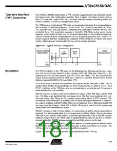
Various communication configurations can be designed using this bus. Figure 131
shows a typical TWI bus configuration using the AT8xC51SND2C in master and slave
modes. All the devices connected to the bus can be master and slave.
Figure 131. Typical TWI Bus Configuration
HOST
Microprocessor
AT8xC51SND2C
Master/Slave
LCD
Display
Audio
DAC
Rp Rp
SCL
SDA
SCL
SDA
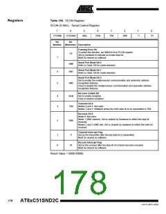
Description
The CPU interfaces to the TWI logic via the following four 8-bit special function regis-
ters: the Synchronous Serial Control register (SSCON SFR, see Table 174), the
Synchronous Serial Data register (SSDAT SFR, see Table 176), the Synchronous
Serial Status register (SSSTA SFR, see Table 175) and the Synchronous Serial
Address register (SSADR SFR, see Table 177).
SSCON is used to enable the controller, to program the bit rate (see Table 174), to
enable slave modes, to acknowledge or not a received data, to send a START or a
STOP condition on the TWI bus, and to acknowledge a serial interrupt. A hardware
reset disables the TWI controller.
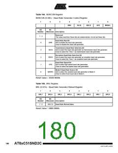
SSSTA contains a status code which reflects the status of the TWI logic and the TWI
bus. The three least significant bits are always zero. The five most significant bits con-
tains the status code. There are 26 possible status codes. When SSSTA contains F8h,
no relevant state information is available and no serial interrupt is requested. A valid sta-
tus code is available in SSSTA after SSI is set by hardware and is still present until SSI
has been reset by software. Table 167 to Table 136 give the status for both master and
slave modes and miscellaneous states.
SSDAT contains a Byte of serial data to be transmitted or a Byte which has just been
received. It is addressable while it is not in process of shifting a Byte. This occurs when
TWI logic is in a defined state and the serial interrupt flag is set. Data in SSDAT remains
stable as long as SSI is set. While data is being shifted out, data on the bus is simulta-
neously shifted in; SSDAT always contains the last Byte present on the bus.
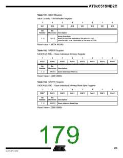
SSADR may be loaded with the 7 - bit slave address (7 most significant bits) to which
the controller will respond when programmed as a slave transmitter or receiver. The
LSB is used to enable general call address (00h) recognition.
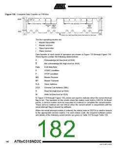
Figure 132 shows how a data transfer is accomplished on the TWI bus.
181
4341D–MP3–04/05

 ATMEL [ ATMEL ]