Application Notes
ATH Series of Wide-Output Adjust Power
Modules (3.3/5-V Input)
Output On/Off Inhibit
Remote Sense
For applications requiring output voltage on/off control,
each series of the ATH family incorporates an output
Inhibit control pin. The inhibit feature can be used wher-
ever there is a requirement for the output voltage from
the regulator to be turned off.
The ATH10, ATH12/15, ATH18/22, and ATH26/30
products incorporate an output voltage sense pin,
Vo Sense. The Vo Sense pin should be connected to Vout at the
load circuit (see data sheet standard application). A re-
mote sense improves the load regulation performance of
the module by allowing it to compensate for any ‘IR’ voltage
drop between itself and the load. An IR drop is caused by
the high output current flowing through the small
amount of pin and trace resistance. Use of the remote
sense is optional. If not used, the Vo Sense pin can be left
open-circuit. An internal low-value resistor (15-Ω or
less) is connected between the Vo Sense and Vout. This en-
sures the output voltage remains in regulation.
The power modules function normally when the Inhibit
pin is left open-circuit, providing a regulated output
whenever a valid source voltage is connected to Vin with
respect to GND.
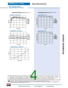
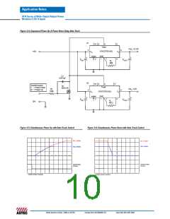
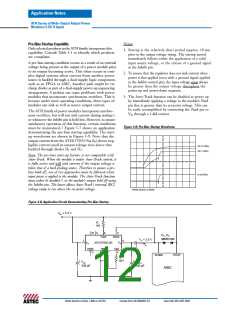
Figure 3-2 shows the typical application of the inhibit
function. Note the discrete transistor (Q1). The Inhibit
control has its own internal pull-up to Vin potential. The
input is not compatible with TTL logic devices. An open-
collector (or open-drain) discrete transistor is recommended
for control.
With the sense pin connected, the difference between
the voltage measured directly between the Vout and GND
pins, and that measured from Vo Sense to GND, is the
amount of IR drop being compensated by the regulator.
This should be limited to a maximum of 0.3 V.
Turning Q1 on applies a low voltage to the Inhibit control
pin and disables the output of the module. If Q1 is then
turned off, the module will execute a soft-start power-up
sequence. A regulated output voltage is produced within
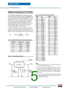
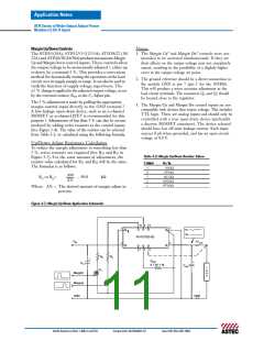
20 msec. Figure 3-3 shows the typical rise in both the
output voltage and input current, following the turn-off
of Q1. The turn off of Q1 corresponds to the rise in the
waveform, Q1 Vds. The waveforms were measured with
Note: The remote sense feature is not designed to compensate
for the forward drop of non-linear or frequency dependent
components that may be placed in series with the converter
output. Examples include OR-ing diodes, filter inductors,
ferrite beads, and fuses. When these components are enclosed
by the remote sense connection they are effectively placed
inside the regulation control loop, which can adversely affect
the stability of the regulator.
a 5-A load.
Figure 3-2
Vo Sense
Over-Temperature Protection
10
9
8
5
The ATH18/22 and ATH26/30 series of products have
over-temperature protection. These products have an
on-board temperature sensor that protects the module’s
internal circuitry against excessively high temperatures.
A rise in the internal temperature may be the result of a
drop in airflow, or a high ambient temperature. If the
internal temperature exceeds the OTP threshold, the
module’s Inhibit control is automatically pulled low. This
turns the output off. The output voltage will drop as the
external output capacitors are discharged by the load
circuit. The recovery is automatic, and begins with a
soft-start power up. It occurs when the the sensed tem-
perature decreases by about 10 °C below the trip point.
VIN
VOUT
2
6
ATH15T05-9S
PTH05020W
3
1
7
4
+
+
L
O
A
D
CIN
1,000 µF
COUT
330 µF
RSET
Q1
BSS138
1 =Inhibit
GND
GND
Figure 3-3
Note: The over-temperature protection is a last resort mecha-
nism to prevent thermal stress to the regulator. Operation at
or close to the thermal shutdown temperature is not recom-
mended and will reduce the long-term reliability of the module.
Always operate the regulator within the specified Safe Operating
Area (SOA) limits for the worst-case conditions of ambient
temperature and airflow.
Vo (2V/Div)
Iin (2A/Div)
Q1Vds (5V/Div)
HORIZ SCALE: 10ms/Div
North America (USA): 1-888-41-ASTEC
Europe (UK): 44(1384)842-211
Asia (HK): 852-2437-9662

 ASTEC [ Astec America, Inc ]