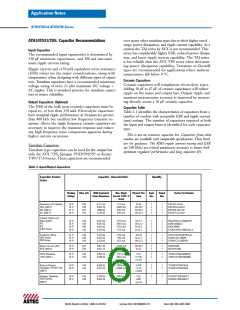
Application Notes
ATH Series of Wide-Output Adjust Power
Modules (3.3/5-V Input)
Margin Up/Down Controls
Notes:
The ATH10 (10A), ATH12/15 (12/15A), ATH18/22 (18/
22A) and ATH26/30 (26/30A) products incorporate Margin
Up and Margin Down control inputs. These controls allow
1. The Margin Up* and Margin Dn* controls were not
intended to be activated simultaneously. If they are
their affects on the output voltage may not completely
cancel, resulting in the possibility of a slightly higher
error in the output voltage set point.
1
the output voltage to be momentarily adjusted , either up
or down, by a nominal 5 %. This provides a convenient
method for dynamically testing the operation of the load
circuit over its supply margin or range. It can also be used to
verify the function of supply voltage supervisors. The
5 % change is applied to the adjusted output voltage, as set
by the external resistor, Rset at the Vo Adjust pin.
2. The ground reference should be a direct connection to
the module GND at pin 7 (pin 1 for the ATH06).
This will produce a more accurate adjustment at the
load circuit terminals. The transistors Q1 and Q2 should
be located close to the regulator.
The 5 % adjustment is made by pulling the appropriate
margin control input directly to the GND terminal .
3. The Margin Up and Margin Dn control inputs are not
compatible with devices that source voltage. This includes
TTL logic. These are analog inputs and should only be
controlled with a true open-drain device (preferably
a discrete MOSFET transistor). The device selected
should have low off-state leakage current. Each input
sources 8 µA when grounded, and has an open-circuit
voltage of 0.8 V.
2
A low-leakage open-drain device, such as an n-channel
MOSFET or p-channel JFET is recommended for this
3
purpose . Adjustments of less than 5 % can also be accom-
modated by adding series resistors to the control inputs
(See Figure 3-4). The value of the resistor can be selected
from Table 3-2, or calculated using the following formula.
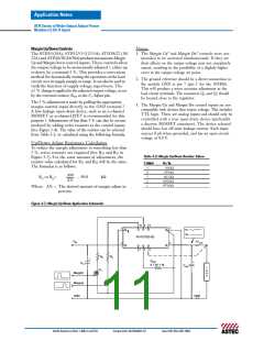
Up/Down Adjust Resistance Calculation
To reduce the margin adjustment to something less than
5 %, series resistors are required (See RD and RU in
Figure 3-7). For the same amount of adjustment, the
resistor value calculated for RU and RD will be the same.
The formulas is as follows.
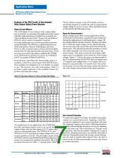
Table 3-2; Margin Up/Down Resistor Values
% Adjust
RU / RD
0.0 kΩ
5
4
3
2
1
24.9 kΩ
66.5 kΩ
499
∆%
RU or RD=
– 99.8
kΩ
150.0 kΩ
397.0 kΩ
Where ∆% = The desired amount of margin adjust in
percent.
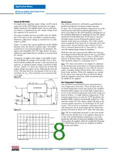
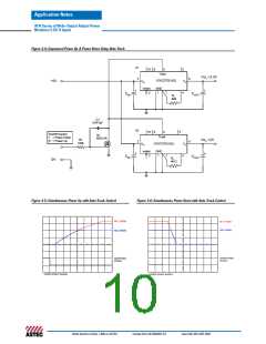
Figure 3-7; Margin Up/Down Application Schematic
10
9
8
1
7
6
+Vo
0V
PTH05010W
ATH15T05-9S
(Top View)
VIN
+VOUT
2
3
4
5
RD
RU
+
RSET
0.1 W, 1 %
+
Cin
MargDn
MargUp
Cout
L
O
A
D
Q1
Q2
GND
GND
North America (USA): 1-888-41-ASTEC
Europe (UK): 44(1384)842-211
Asia (HK): 852-2437-9662

 ASTEC [ Astec America, Inc ]