ATH10T05 Series —5-V Input
10-A, 5-V Input Non-Isolated
Wide-Output Adjust Power Module
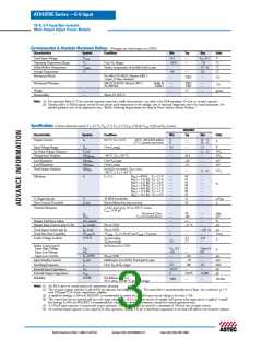
Environmental & Absolute Maximum Ratings (Voltages are with respect to GND)
Characteristics
Symbols
Conditions
Min
Typ
Max
Units
Track Input Voltage
Vtrack
–0.3
—
—
Vin + 0.3
85
V
(i)
Operating Temperature Range
Solder Reflow Temperature
Storage Temperature
T
Over V Range
Surface temperature of module body or pins
—
Per Mil-STD-883D, Method 2002.3
1 msec, ½ Sine, mounted
–40
°C
°C
°C
a
in
(ii)
Treflow
T
s
215
–40
—
—
125
Mechanical Shock
TBD
—
G’s
Mechanical Vibration
Mil-STD-883D, Method 2007.2
20-2000 Hz
Suffix H
Suffix S
—
—
TBD
TBD
—
—
G’s
Weight
Flammability
—
—
—
3.7
—
grams
Meets UL 94V-O
Notes: (i) For operation below 0 °C the external capacitors must bave stable characteristics. use either a low ESR tantalum, Os-Con, or ceramic capacitor.
(ii) During reflow of SMD package version do not elevate peak temperature of the module, pins or internal components above the stated maximum. For
further guidance refer to the application note, “Reflow Soldering Requirements for Plug-in Power Surface Mount Products.”
Specifications (Unless otherwise stated, Ta =25 °C, Vin =5 V, Vo =3.3 V, Cin =330 µF, Cout =0 µF, and Io =Iomax)
ATH10T05
Characteristics
Symbols
Conditions
Min
Typ
Max
Units
(1)
(1)
Output Current
Io
0.8 V ≤ Vo ≤ 3.6 V,
60 °C, 200 LFM airflow
25 °C, natural convection
0
0
—
—
10
10
A
Input Voltage Range
Set-Point Voltage Tolerance
Temperature Variation
Line Regulation
Load Regulation
Total Output Variation
Vin
Vo tol
∆Regtemp
∆Regline
∆Regload
∆Regtot
Over Io range
4.5
—
—
—
—
—
—
0.5
10
12
5.5
2
—
—
—
V
(2)
%Vo
%Vo
mV
mV
–40 °C <Ta < +85 °C
Over Vin range
Over Io range
Includes set-point, line, load,
(2)
—
—
3
%Vo
–40 °C ≤ Ta ≤ +85 °C
Efficiency
η
Io =7 A
RSET = 698 Ω Vo = 3.3 V
—
—
—
—
—
—
—
94
92
91
90
89
86
85
—
—
—
—
—
—
—
RSET = 2.21 kΩ Vo = 2.5 V
RSET = 4.12 kΩ Vo = 2.0 V
RSET = 5.49 kΩ Vo = 1.8 V
RSET = 8.87 kΩ Vo = 1.5 V
RSET = 17.4 kΩ Vo = 1.2 V
RSET = 36.5 kΩ Vo = 1.0 V
%
Vo Ripple (pk-pk)
Over-Current Threshold
Transient Response
Vr
Io trip
20 MHz bandwidth
Reset, followed by auto-recovery
1 A/µs load step, 50 to 100 % Iomax,
Cout =330 µF
—
—
25
20
—
—
mVpp
A
ttr
Recovery Time
Vo over/undershoot
—
—
70
—
—
µSec
mV
∆Vtr
100
Margin Up/Down Adjust
Margin Input Current (pins 9 /10)
Track Input Current (pin 8)
Track Slew Rate Capability
Under-Voltage Lockout
∆Vo margin
IIL margin
IIL track
dVtrack/dt
UVLO
—
—
—
5
5
– 8
—
—
4.3
3.7
—
—
–130
—
4.45
—
%
µA
µA
V/ms
(3)
Pin to GND
Pin to GND
Vtrack – Vo ≤ 50 mV and Vtrack < Vo(nom)
Vin increasing
Vin decreasing
Referenced to GND
(4)
(4)
—
V
V
3.4
Inhibit Control (pin3)
Input High Voltage
Input Low Voltage
VIH
VIL
Vin –0.5
–0.2
—
—
Open
0.6
IIL inhibit
Input Low Current
Input Standby Current
Switching Frequency
External Input Capacitance
External Output Capacitance
Reliability
Pin to GND
Inhibit (pin 3) to GND, Track (pin 8) open
Over Vin and Io ranges
—
—
275
330
–130
10
300
—
—
—
325
—
15,000
µA
Iin inh
ƒs
Cin
Cout
MTBF
mA
kHz
µF
(5)
(6)
0
330
µF
Per Bellcore TR-332
6
TBD
—
—
10 Hrs
50 % stress, Ta =40 °C, ground benign
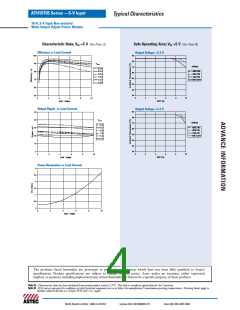
Notes: (1) See SOA curves or consult factory for appropriate derating.
(2) The set-point voltage tolerance is affected by the tolerance and stability of RSET. The stated limit is unconditionally met if RSET has a tolerance of 1 %
with 100 ppm/°C or better temperature stability.
(3) A small low-leakage (<100 nA) MOSFET is recommended to control this pin. The open-circuit voltage is less than 1 Vdc.
(4) This control pin has an internal pull-up to the input voltage Vin. If it is left open-circuit the module will operate when input power is applied. A small
low-leakage (<100 nA) MOSFET is recommended for control. For further information, consult the related application note.
(5) A 330 µF input capacitor is required for proper operation. The capacitor must be rated for a minimum of 500 mA rms of ripple current.
(6) An external output capacitor is not required for basic operation. Adding 330 µF of distributed capacitance at the load will improve the transient response.
North America (USA): 1-888-41-ASTEC
Europe (UK): 44(1384)842-211
Asia (HK): 852-2437-9662

 ASTEC [ Astec America, Inc ]