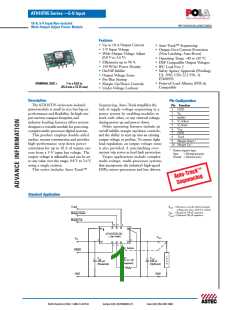
ATH10T05 Series —5-V Input
10-A, 5-V Input Non-Isolated
Wide-Output Adjust Power Module
REVISION 00 (4DEC2003)
Ordering Information
Input Voltage
4.5V to 5.5V
Output Voltage
0.8V1 to 3.6V
Output Current
10A
Model Number
ATH10T05-9(S)(J)
Options:
“-J”
-
-
-
Through-hole Termination, Tray Packaging
SMT Termination, Tray Packaging
SMT Termination, T&R Packaging
“-SJ”
“-S”
Notes:
1Preset output voltage is 0.8V; externally adjustable to 3.6V through the Vo,Adjust pin
Pin Descriptions
Vin: The positive input voltage power node to the mod-
ule, which is referenced to common GND.
Vo Sense: The sense input allows the regulation circuit to
compensate for voltage drop between the module and
the load. For optimal voltage accuracy Vo Sense should
be connected to Vout. It can also be left disconnected.
Vout: The regulated positive power output with respect
to the GND node.
Track: This is an analog control input that enables the
output voltage to follow an external voltage. This pin
becomes active typically 20 ms after the input voltage
has been applied, and allows direct control of the output
voltage from 0 V up to the nominal set-point voltage.
Within this range the output will follow the voltage at
the Track pin on a volt-for-volt basis. When the control
voltage is raised above this range, the module regulates
at its set-point voltage. The feature allows the output
voltage to rise simultaneously with other modules pow-
ered from the same input bus. If unused, the input may
be left unconnected. Note: Due to the under-voltage lockout,
this feature does not allow the output from the module to follow
its own input voltage during power up. For more information,
consult the related application note.
GND: This is the common ground connection for the
Vin and Vout power connections. It is also the 0 VDC
reference for the control inputs.
Inhibit: The Inhibit pin is an open-collector/drain negative
logic input that is referenced to GND. Applying a low-
level ground signal to this input disables the module’s
output and turns off the output voltage. When the Inhibit
control is active, the input current drawn by the regula-
tor is significantly reduced. If the Inhibit pin is left
open-circuit, the module will produce an output when-
ever a valid input source is applied.
Vo Adjust: A 0.1 W 1 % resistor must be directly connected
between this pin and pin 7 (GND) to set the output voltage
to a value higher than 0.8 V. The temperature stability of
the resistor should be 100 ppm/°C (or better). The set
point range for the output voltage is from 0.8 V to 3.6 V.
The resistor value required for a given output voltage
may be calculated from the following formula. If left
open circuit, the output voltage will default to its lowest
value. For further information on output voltage adjust-
ment consult the related application note.
Margin Down: When this input is asserted to GND, the
output voltage is decreased by 5% from the nominal. The
input requires an open-collector (open-drain) interface.
It is not TTL compatible. A lower percent change can
be accomodated with a series resistor. If unused, the
input may be left unconnected. For further information,
consult the related application note.
Margin Up: When this input is asserted to GND, the output
voltage is increased by 5%. The input requires an open-
collector (open-drain) interface. It is not TTL compatible.
The percent change can be reduced with a series resistor. If
unused, the input may be left unconnected. For further
information, consult the related application note.
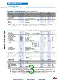
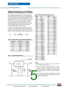
0.8 V
Vout – 0.8 V
Rset
= 10 kΩ
– 2.49 kΩ
The specification table gives the preferred resistor values
for a number of standard output voltages.
North America (USA): 1-888-41-ASTEC
Europe (UK): 44(1384)842-211
Asia (HK): 852-2437-9662

 ASTEC [ Astec America, Inc ]