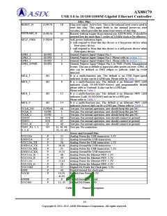
AX88179
USB 3.0 to 10/100/1000M Gigabit Ethernet Controller
3.7 USB to Ethernet Bridge
The USB to Ethernet bridge block is responsible for converting Ethernet MAC frame into USB packets or vice-versa. This
block supports proprietary burst transfer mechanism (US Patent Approval) to offload software burden and to offer very high
packet transfer throughput over USB bus.
This USB to Ethernet bridge block not only co-work with “eFuse and Control”, “SEEPROM Loader I/F”, and General
Purpose I/Os and LEDs, but also handle USB Control transfers of Endpoint 0.
3.8 eFuse and Control
The eFuse (64-byte) and Control supports user to program USB descriptions and some device information. The data format
is shown at Section 4.
3.9 SEEPROM Loader Interface
The SEEPROM loader interface is responsible for reading configuration data automatically from the external serial
EEPROM or eFuse after power-on reset.
If the content of EEPROM offset 05h (low byte) was equal to (0xFF - SUM [EEPROM offset 03h ~ 04h]), the EEPROM is
the first candidate for SEEEPROM loader. If failed checksum checking the eFuse will be the second candidate.
If this SEEPROM Loader checks the 1st byte data of efuse is not equal to 0xFF and the eFuse Checksum [7:0] of eFuse
offset 19h is correct, the content of eFuse is valid for SEEPROM loader. If eFuse Checksum [7:0] is incorrect, the chip’s
internal default setting will be brought up to configure the corresponding valus and respond to USB standard commands,
etc.
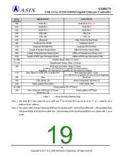
3.10 General Purpose I/O and LED
There are 4 general-purpose I/O pins (named GPIO_0/1/2/3) and 4 multi-function pins group A (named MFA_0/1/2/3)
provided by this chip. The MFA_0/1/2/3 pins are also used for LED indication. Please refer to Section 4.1.6 for details.
14
Copyright © 2011-2012 ASIX Electronics Corporation. All rights reserved.

 ASIX [ ASIX ELECTRONICS CORPORATION ]