AX88179
USB 3.0 to 10/100/1000M Gigabit Ethernet Controller
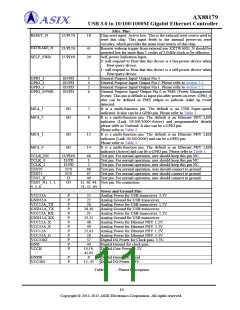
Misc. Pins
RESET_N
I5/PU/S
18
Chip reset input. Active low. This is the external reset source used to
reset this chip. This input feeds to the internal power-on reset
circuitry, which provides the main reset source of this chip.
Remote-wakeup trigger from external pin. EXTWAKE_N should be
asserted low for more than 2 cycles of 25MHz clock to be effective.
Self_power Indication Input.
EXTWAKE_N
SELF_PWR
I3/PU/S
I5/PD/S
41
20
0: will respond to Host that this device is a bus-power-device when
Host query device.
1: will respond to Host that this device is a self-power-device when
Host query device.
GPIO_3
GPIO_2
GPIO_1
GPIO_0/PME
B3/PD
B3/PD
B3/PD
B3/PD
3
4
5
6
General Purpose Input/ Output Pin 3.
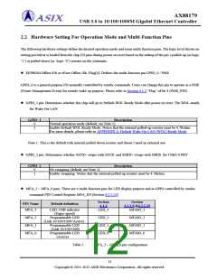
General Purpose Input/ Output Pin 2. Please refer to section 2.2.
General Purpose Input/ Output Pin 1. Please refer to section 2.2.
General Purpose Input/ Output Pin 0 or PME (Power Management
Event). This pin is default as input pin after power-on reset. GPIO_0
also can be defined as PME output to indicate wake up event
detected.
MFA_3
MFA_2
B3
B3
7
8
It is a multi-function pin. The default is an USB Super-speed
indicator. It also can be a GPIO pin. Please refer to Table 2.
It is a multi-function pin. The default is an Ethernet PHY LED
indicator (Link 10/100/1000+Active) and programmable details
please refer to Vndcmd. It also can be a GPIO pin.
Please refer to Table 2.
MFA_1
MFA_0
B3
B3
13
14
It is a multi-function pin. The default is an Ethernet PHY LED
indicator (Link 10/100/1000) and can be a GPIO pin.
Please refer to Table 2.
It is a multi-function pin. The default is an Ethernet PHY LED
indicator (Active) and can be a GPIO pin. Please refer to Table 2.
Test pin. For normal operation, user should keep this pin NC.
Test pin. For normal operation, user should keep this pin NC.
Test pin. For normal operation, user should keep this pin NC.
Test pin. For normal operation, user should connect to ground.
Test pin. For normal operation, user should connect to ground.
Test pin. For normal operation, user should connect to ground.
TCLK_EN
TCLK_0
TCLK_1
TEST0
I3/PD/S
I3/PD
I3/PD
I3/S
I3/S
I3
68
1
2
66
67
46
TEST1
TEST_X
TEST_N1, 2, 3,
4, 5, 6
O3
11, 36, 44, Test pin. No connection
51, 52, 64
Power and Ground Pins
VCC33A
GND33A
P
P
P
P
P
P
P
P
P
P
P
P
P
25
22
26
28,30
31
33,35
48
49
55,61
58
37
40
Analog Power for USB transceiver. 3.3V.
Analog Ground for USB transceiver.
Analog Power for USB transceiver. 1.2V.
Analog Ground for USB transceiver.
Analog Power for USB transceiver. 1.2V.
Analog Ground for USB transceiver.
Analog Power for Ethernet PHY. 1.2V.
Analog Power for Ethernet PHY. 3.3V.
Analog Power for Ethernet PHY. 1.2V.
Analog Power for Ethernet PHY. 3.3V.
Digital I/O Power for Clock pins. 3.3V.
Digital Ground for clock pins.
VCC12A_TX
GND12A_TX
VCC12A_RX
GND12A_RX
VCC12A_X
VCC33A_X
VCC12A
VCC33A_G
VCC33IO
GND
VCCK
10,19,
45,65
9
Digital Core Power. 1.2V.
GNDK
VCC3IO
P
P
Digital Ground to E-pad
Digital I/O Power. 3.3V.
12, 43
Table 1
: Pinout Description
10
Copyright © 2011-2012 ASIX Electronics Corporation. All rights reserved.

 ASIX [ ASIX ELECTRONICS CORPORATION ]