AX88179
USB 3.0 to 10/100/1000M Gigabit Ethernet Controller
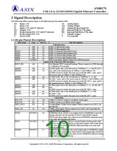
2 Signal Description
The following abbreviations apply to the following pin description table.
I12 Input, 1.2V AI Analog Input
I3
Input, 3.3V
AO Analog Output
I5
Input, 3.3V with 5V tolerant
Output, 3.3V
Bi-directional I/O, 3.3V with 5V tolerant
Bi-directional I/O, 3.3V
Power/GND
AB Analog Bi-directional I/O
O3
B5
B3
P
PU
PD
S
Internal Pull Up (75K ohm)
Internal Pull Down (75K ohm)
Schmitt Trigger
T
Tri-stateable
2.1 68-pin Pinout Description
Pin Name
Type
Pin No
Pin Description
USB Interface
D+
D-
AB
AB
AB
AB
AB
23
24
29
27
34
32
21
USB 2.0 data positive pin.
USB 2.0 data negative pin.
SSTX+
SSTX-
SSRX+
SSRX-
VBUS
USB 3.0 transmit data positive pin.
USB 3.0 transmit data negative pin.
USB 3.0 receive data positive pin.
USB 3.0 receive data negative pin.
VBUS pin input. Please connect to USB bus power.
AB
I5/PD/S
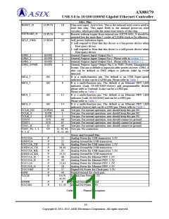
Gigabit EEE Ethernet PHY Interface
RSET_BG
AO
47
For Ethernet PHY’s internal biasing. Please connect to GND through
a 2.49Kohm ±1% resistor.
MDIP0
MDIN0
AB
AB
53
54
In MDI mode, this is the first pair in 1000Base-T, i.e. the BI_DA+/-
pair, and is the transmit pair in 10Base-T and 100Base-TX.
In MDI crossover mode, this pair acts as the BI_DB+/- pair, and is
the receive pair in 10Base-T and 100Base-TX.
In MDI mode, this is the second pair in 1000Base-T, i.e. the
BI_DB+/- pair, and is the receive pair in 10Base-T and 100Base-TX.
In MDI crossover mode, this pair acts as the BI_DA+/- pair, and is
the transmit pair in 10Base-T and 100Base-TX.
In MDI mode, this is the third pair in 1000Base-T, i.e., the BI_DC+/-
pair.
MDIP1
MDIN1
AB
AB
56
57
MDIP2
MDIN2
AB
AB
59
60
In MDI crossover mode, this pair acts as the BI_DD+/- pair.
In MDI mode, this is the fourth pair in 1000Base-T, i.e., the
BI_DD+/- pair.
MDIP3
MDIN3
AB
AB
62
63
In MDI crossover mode, this pair acts as the BI_DC+/- pair.
Clock Pins
XTL25P
I3
38
25Mhz ± 0.005% crystal or oscillator clock input.
XTL25N
CK25_OUT
O3
O3
39
42
25Mhz crystal or oscillator clock output.
A controllable 25Mhz clock output. Please connect it to CK25_IN
pin directly.
CK25_IN
EECK
I3
50
16
25Mhz clock input. Please connect it to CK25_OUT pin directly.
Serial EEPROM Interface
EEPROM Clock. EECK is an output clock to EEPROM to provide
timing reference for the transfer of EECS, and EEDIO signals.
EECK only drive high / low when access EEPROM otherwise keep
at tri-state and internal pull-down.
B5/PD/T
EECS
B5/PD/T
B5/PU/T
17
15
EEPROM Chip Select. EECS is asserted high synchronously with
respect to rising edge of EECK as chip select signal. EECS only drive
high / low when access EEPROM otherwise keep at tri-state and
internal pull-down.
EEPROM Data. EEDIO is the serial output data to EEPROM’s data
input pin and is synchronous with respect to the rising edge of EECK.
EEDIO only drive high / low when access EEPROM otherwise keep
at tri-state and internal pull-up.
EEDIO
9
Copyright © 2011-2012 ASIX Electronics Corporation. All rights reserved.

 ASIX [ ASIX ELECTRONICS CORPORATION ]