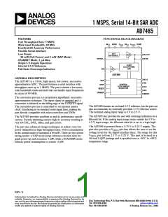
AD7485
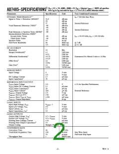
Parameter
Specification
Unit
Test Conditions/Comments
POWER REQUIREMENTS
VDD
5
V
5%
VDRIVE
2.7
5.25
V min
V max
IDD
Normal Mode (Static)
Normal Mode (Operational)
NAP Mode
12
16
0.6
2
mA max
mA max
mA max
µA max
µA typ
STANDBY Mode8
0.5
Power Dissipation
Normal Mode (Operational)
NAP Mode
80
3
10
mW max
mW max
µW max
STANDBY Mode8
NOTES
1Temperature ranges as follows: –40°C to +85°C.
2SINAD figures quoted include external analog input circuit noise contribution of approximately 1 dB.
3See Typical Performance Characteristics section for analog input circuits used.
4See Terminology.
5Sample tested @ 25°C to ensure compliance.
6Current drawn from external reference during conversion.
7ILOAD = 200 µA.
8Digital input levels at GND or VDRIVE
.
Specifications subject to change without notice.
(VDD = 5 V ꢁ 5%, AGND = DGND = 0 V, VREF = External; all specifications TMIN to TMAX and
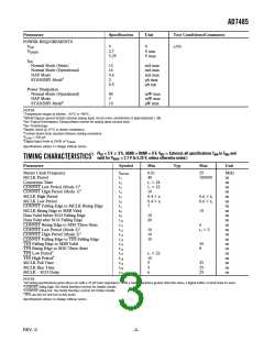
TIMING CHARACTERISTICS1
valid for VDRIVE = 2.7 V to 5.25 V, unless otherwise noted.)
Parameter
Symbol
Min
Typ
Max
Unit
Master Clock Frequency
MCLK Period
fMCLK
t1
t2
t3
t4
t5
t6
t7
t8
0.01
40
25
100000
MHz
ns
ns
ns
ns
ns
ns
ns
ns
ns
ns
ns
ns
ns
ns
ns
ns
ns
ns
ns
ns
ns
Conversion Time
t1 ꢁ 24
t1 ꢁ 22
10
0.4 ꢁ t1
0.4 ꢁ t1
7
CONVST Low Period (Mode 1)2
CONVST High Period (Mode 1)2
MCLK High Period
0.6 ꢁ t1
0.6 ꢁ t1
MCLK Low Period
CONVST Falling Edge to MCLK Rising Edge
MCLK Rising Edge to MSB Valid
Data Valid before SCO Falling Edge
Data Valid after SCO Falling Edge
CONVST Rising Edge to SDO Three-State
CONVST Low Period (Mode 2)2
CONVST High Period (Mode 2)3
CONVST Falling Edge to TFS Falling Edge
TFS Falling Edge to MSB Valid
TFS Rising Edge to SDO Three-State
TFS Low Period4
15
t9
10
20
t10
t11
t12
t13
t14
t15
t16
t17
t18
t19
t20
t21
6
10
10
10
t1 ꢁ 2
30
8
t1 ꢁ 22
10
5
5
TFS High Period4
MCLK Fall Time
MCLK Rise Time
MCLK – SCO Delay
25
25
25
6
NOTES
1All timing specifications given above are with a 25 pF load capacitance. With a load capacitance greater than this value, a digital buffer or latch must be used.
2CONVST idling high. See Serial Interface section for further details.
3CONVST idling low. See Serial Interface section for further details.
4TFS can also be tied low in this mode.
Specifications subject to change without notice.
REV. 0
–3–

 AMICC [ AMIC TECHNOLOGY ]