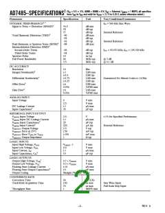
(VDD = 5 V ꢁ 5%, AGND = DGND = 0 V, VREF = External, fSAMPLE = 1 MSPS; all specifica-
AD7485–SPECIFICATIONS1 tions TMIN to TMAX and valid for VDRIVE = 2.7 V to 5.25 V, unless otherwise noted.)
Parameter
Specification
Unit
Test Conditions/Comments
DYNAMIC PERFORMANCE2, 3
fIN = 500 kHz Sine Wave
Signal to Noise + Distortion (SINAD)4
76.5
78
77
–90
–95
–92
–88
dB min
dB typ
dB typ
dB max
dB typ
dB typ
dB max
Internal Reference
Total Harmonic Distortion (THD)4
Internal Reference
Peak Harmonic or Spurious Noise (SFDR)4
Intermodulation Distortion (IMD)4
Second-Order Terms
Third-Order Terms
Aperture Delay
–96
–94
10
dB typ
dB typ
ns typ
fIN1 = 95.053 kHz, fIN2 = 105.329 kHz
Full Power Bandwidth
40
3.5
MHz typ
MHz typ
@ 3 dB
@ 0.1 dB
DC ACCURACY
Resolution
14
1
0.5
0.75
0.25
6
0.036
6
0.036
Bits
Integral Nonlinearity4
LSB max
LSB typ
LSB max
LSB typ
LSB max
%FSR max
LSB max
%FSR max
Differential Nonlinearity4
Offset Error4
Guaranteed No Missed Codes to 14 Bits
Gain Error4
ANALOG INPUT
Input Voltage
0
2.5
1
V min
V max
µA max
pF typ
DC Leakage Current
Input Capacitance5
35
REFERENCE INPUT/OUTPUT
V
REFIN Input Voltage
2.5
1
V
1% for Specified Performance
External Reference
VREFIN Input DC Leakage Current
V
V
VREFOUT Output Voltage
V
V
µA max
pF typ
ꢀA typ
V typ
mV typ
mV max
Ω typ
REFIN Input Capacitance5
REFIN Input Current6
25
220
2.5
50
100
1
REFOUT Error @ 25°C
REFOUT Error TMIN to TMAX
VREFOUT Output Impedance
LOGIC INPUTS
Input High Voltage, VINH
Input Low Voltage, VINL
Input Current, IIN
VDRIVE –1
0.4
1
V min
V max
µA max
pF typ
5
Input Capacitance, CIN
10
LOGIC OUTPUTS
7
Output High Voltage, VOH7
0.7 × VDRIVE
V min
Output Low Voltage, VOL
Floating-State Leakage Current
Floating-State Output Capacitance5
Output Coding
0.3 × VDRIVE
V max
µA max
pF max
10
10
Straight (Natural) Binary
CONVERSION RATE
Conversion Time
Track/Hold Acquisition Time
24
100
70
1
MCLKs
ns max
ns max
MSPS max
Sine Wave Input
Full-Scale Step Input
Throughput Rate
–2–
REV. 0

 AMICC [ AMIC TECHNOLOGY ]