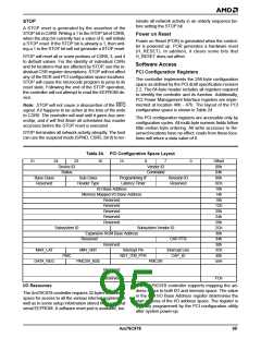
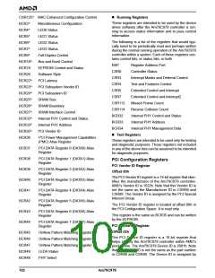
Table 27. I/O Map in DWord I/O Mode (DWIO = 1)
IEEE 802.3, Section 14.3.1.2. The load is a twisted pair
cable that meets IEEE 802.3, Section 14.4.
The TX± signal is filtered on the chip to reduce har-
monic content per Section 14.3.2.1 (10BASE-T). Since
filtering is performed in silicon, TX± can be connected
directly to a standard transformer. External filtering
modules are not needed.
Offset
00h - 0Fh
10h
No. of Bytes
Register
APROM
RDP
16
4
RAP (shared by RDP and
BDP)
14h
4
Twisted Pair Receive Function
18h
1Ch
4
4
Reset Register
BDP
The RX+ port is a differential twisted-pair receiver.
When properly terminated, the RX+ port will meet the
electrical requirements for 10BASE-T receivers as
specified in IEEE 802.3, Section 14.3.1.3. The receiver
has internal filtering and does not require external filter
modules or common mode chokes.
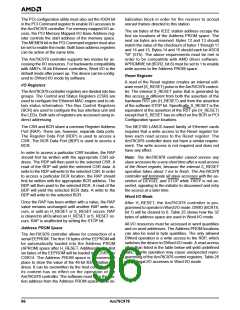
Table 28. Legal I/O Accesses in Double Word I/O
Mode (DWIO =1)
AD[4:0]
BE[3:0]
Type
Comment
Signals appearing at the RX± differential input pair are
routed to the internal decoder. The receiver function
meets the propagation delays and jitter requirements
specified by the 10BASE-T standard. The receiver
squelch level drops to half its threshold value after un-
squelch to allow reception of minimum amplitude sig-
nals and to mitigate carrier fade in the event of worst
case signal attenuation and crosstalk noise conditions.
DWord read of APROM
locations 3h (MSB) to 0h
RD (LSB),
7h to 4h, Bh to 8h, or Fh to
0XX00
0000
Ch
10000
10100
0000
0000
RD DWord read of RDP
RD DWord read of RAP
DWord read of Reset
Register
11000
0000
RD
DWord write to APROM
locations 3h (MSB) to 0h
WR (LSB),
Clock
Data
Clock
Data
0XX00
0000
7h to 4h, Bh to 8h, or Fh to
Ch
Manchester
Encoder
Manchester
Decoder
10000
10100
0000
0000
WR DWord write to RDP
WR DWord write to RAP
DWord write to Reset
Register
11000
0000
WR
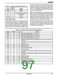
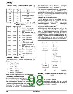
10BASE-T Physical Layer
Squelch
Circuit
The 10BASE-T block consists of the following sub-
blocks:
— Transmit Process
— Receive Process
TX Driver
TX±
RX Driver
RX±
— Interface Status
— Collision Detect Function
— Jabber Function
22206B-54
— Reverse Polarity Detect
Refer to Figure 50 for the 10BASE-T block diagram.
Figure 50. 10BASE-T Transmit and Receive Data
Paths
Twisted Pair Transmit Function
Data transmission over the 10BASE-T medium re-
quires use of the integrated 10BASE-T MAU and uses
the differential driver circuitry on the TX± pins.
Twisted Pair Interface Status
The Am79C978 device will power up in the Link Fail
state. The Auto-Negotiation algorithm will apply to
allow it to enter the Link Pass state.
TX± is a differential twisted-pair driver. When properly
terminated, TX± will meet the transmitter electrical re-
quirements for 10BASE-T transmitters as specified in
98
Am79C978

 AMD [ AMD ]