The following is a list of the registers that would typi-
cally need to be programmed once during the setup of
the controller within a system. The control bits in each
of these registers typically do not need to be modified
once they have been written. However, there are no re-
strictions as to how many times these registers may ac-
tually be accessed. Note that if the default power up
values of any of these registers is acceptable to the ap-
plication, then such registers need never be accessed
at all.
USER ACCESSIBLE REGISTERS
The Am79C978 controller has four types of user regis-
ters: the PCI configuration registers, the Control and
Status registers (CSRs), the Bus Control registers
(BCRs), 10BASE-T PHY Management registers
(TBRs), and 1 Mbps HomePNA PHY Management reg-
isters (HPRs).
The Am79C978 controller implements all PCnet-ISA
(Am79C960) registers, all C-LANCE (Am79C90) regis-
ters, plus a number of additional registers. The
Am79C978 CSRs are compatible upon power up with
both the PCnet-ISA CSRs and all of the C-LANCE
CSRs.
Note: Registers marked with “^” may be programma-
ble through the EEPROM read operation and, there-
fore, do not necessarily need to be written to by the
system initialization procedure or by the driver soft-
ware. Registers marked with “*” will be initialized by the
initialization block read operation.
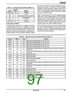
The PCI configuration registers can be accessed in any
data width. All other registers must be accessed ac-
cording to the I/O mode that is currently selected.
When WIO mode is selected, all other register loca-
tions are defined to be 16 bits in width. When DWIO
mode is selected, all these register locations are de-
fined to be 32 bits in width, with the upper 16 bits of
most register locations marked as reserved locations
with undefined values. When performing register write
operations in DWIO mode, the upper 16 bits should al-
ways be written as zeros. When performing register
read operations in DWIO mode, the upper 16 bits of
I/O resources should always be regarded as having un-
defined values, except for CSR88.
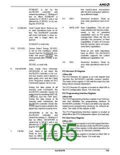
CSR1
Initialization Block Address[15:0]
Initialization Block Address[31:16]
Interrupt Masks and Deferral Control
Test and Features Control
CSR2*
CSR3
CSR4
CSR5
Extended Control and Interrupt
Extended Control and Interrupt2
Logical Address Filter[15:0]
CSR7
CSR8*
CSR9*
CSR10*
CSR11*
Logical Address Filter[31:16]
Logical Address Filter[47:32]
Logical Address Filter[63:48]
The Am79C978 registers can be divided into four
groups: PCI Configuration, Setup, Running, and Test.
Registers not included in any of these categories can
be assumed to be intended for diagnostic purposes.
CSR12*^ Physical Address[15:0]
CSR13*^ Physical Address[31:16]
CSR14*^ Physical Address[47:32]
n PCI Configuration Registers
These registers are intended to be initialized by the
system initialization procedure (e.g., BIOS device ini-
tialization routine) to program the operation of the con-
troller PCI bus interface.
CSR15*
CSR24*
CSR25*
CSR30*
CSR31*
CSR47*
CSR49*
CSR76*
CSR78*
CSR80
Mode
Base Address of Receive Ring Lower
Base Address of Receive Ring Upper
Base Address of Transmit Ring Lower
Base Address of Transmit Ring Upper
Transmit Polling Interval
The following is a list of the registers that would typi-
cally need to be programmed once during the initializa-
tion of the Am79C978 controller within a system:
— PCI I/O Base Address or Memory Mapped I/O
Base Address register
— PCI Expansion ROM Base Address register
— PCI Interrupt Line register
— PCI Latency Timer register
— PCI Status register
Receive Polling Interval
Receive Ring Length
Transmit Ring Length
DMA Transfer Counter and FIFO Thresh-
old Control
— PCI Command register
— OnNow register
CSR82
Bus Activity Timer
n Setup Registers
CSR100
Memory Error Timeout
These registers are intended to be initialized by the de-
vice driver to program the operation of various control-
ler features.
CSR116^ OnNow Miscellaneous
CSR122 Receiver Packet Alignment Control
Am79C978
101

 AMD [ AMD ]